


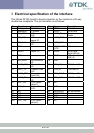
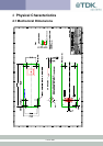

Electrical specification of the interface 3
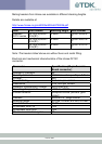
The Hirose DF12C board to board connector on the module is a 40 way
double-row receptacle. The pin allocation is as follows:
Pin Signal Description Pin Signal Description
1 Analogue 0 1.8v Max 2 GPIO1 I/O for Host
3 Analogue 1 1.8v Max 4 GPIO2 I/O for Host
5 SPI_MISO SPI bus serial
O/P
6 UART_RI ‘Ring’ Input or
Output
7 SPI_CSB SPI bus chip
select I/P
8 UART_DCD Input or Output
9 SPI_CLK SPI bus clock
I/P
10 UART_DSR Input
11 GND 12 GPIO3/UART
_DTR
I/O for Host
13 RESET Reset I/P 14 GPIO4 I/O for Host
(Right LED)(2)
15 GND 16 GPIO5 I/O for Host (Left
LED) (2)
17 SPI_MOSI SPI bus serial
I/P
18 GND
19 UART_CTS Clear to Send
I/P
20 PCM_CLK PCM Clock I/P
21 UART_TX Transmit Data
O/P
22 PCM_IN PCM Data I/P
23 UART_RTS Request to
Send O/P
24 PCM_SYNC PCM Sync I/P
25 UART_RX Receive Data
I/P
26 PCM_OUT PCM Data O/P
27 VCC_3V3 3.3V Output
(Note 3)
28 N/C
29 VCC_5V 3.6V < VIN <
6.0V
30 GND
31 N/C 32 RESERVED Do not connect
33 N/C 34 RESERVED Do not connect
35 N/C 36 GND
37 N/C 38 GND
39 VCC_1V8 1.8V Output
(Note 3)
40 N/C
9 of 36