


1DeviceClocking
1.1Overview
1.2ClockDomains
1.2.1CoreDomains
User'sGuide
SPRUES0B–December2007
Phase-LockedLoopController(PLLC)
TheC642xDSPrequiresoneprimaryreferenceclock.Theprimaryreferenceclockcanbeeithercrystal
inputordrivenbyexternaloscillators.A15to30MHZcrystalattheMXI/CLKINpinisrecommendedfor
thesystemPLLs,whichgeneratetheclocksfortheDSP,peripherals,andDMA.
Fordetailedspecificationsonclockfrequencyandvoltagerequirements,seethedevice-specificdata
manual.
Therearetwoclockingmodes:
•PLLBypassMode-powersaving(devicedefaultstothismode)
•PLLMode-PLLmultipliesinputclockuptothedesiredoperatingfrequency
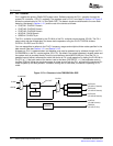
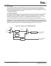
Theclockofthemajorchipcomponentsmustbeprogrammedtooperateatfixedratiosoftheprimary
system/DSPclockfrequencywithineachmode,asshowninTable1.TheC642xDSPclocking
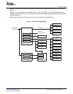
architectureisshowninFigure1.
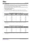
Table1.SystemClockModesandFixedRatiosforCoreClockDomains
ComponentsCoreClockDomainFixedRatiovs.DSPfrequency
DSPCLKDIV11:1
EDMACLKDIV31:3
Peripherals(CLKDIV3domain)CLKDIV31:3
Peripherals(CLKDIV6domain)CLKDIV61:6
ThecoredomainsrefertotheclockdomainsforalloftheinternalprocessingelementsoftheC642xDSP,
suchastheDSP/EDMA/peripherals,etc.AllinternalcommunicationsbetweenDSPandmodulesoperate
atcoredomainclockfrequencies.Allofthecoreclockdomainsaresynchronoustoeachother,comefrom
asinglePLL(PLL1),havealignedclockedges,andhavefixeddividebyratiorequirements,asshownin
Table1andFigure1.Itisuser'sresponsibilitytoensurethefixeddivideratiosbetweenthesecoreclock
domainsareachieved.
TheDSPisintheCLKDIV1domainandreceivesthePLL1frequencydirectly(PLLDIV1ofPLLcontroller
1(PLLC1)settodivideby1),orreceivesthedivided-downPLL1frequency(PLLDIV1ofPLLC1setto
divideby2,3,etc.).TheDSPhasinternalclockdividersthatitusestocreatetheDSP÷3clockfrequency
tocommunicatewithothercomponentson-chip.
ModulesintheCLKDIV3domain(forexample,EDMA,CLKDIV3domainperipherals)mustrunat1/3the
DSPfrequency.
6Phase-LockedLoopController(PLLC)SPRUES0B–December2007
SubmitDocumentationFeedback