


SLUU195 − June 2004
19
TPS40090 Multi-Phase Buck Converter and TPS2834 Drivers Steps-Down from 12-V to 1.5-V at 100 A
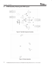
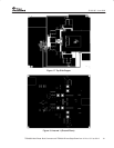
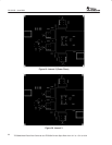
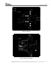
7 Layout Considerations
The PCB layout plays a critical role in the performance in a high frequency switching power
supply design. Following the suggestions listed below will help to improve the performance and
expedite the design.
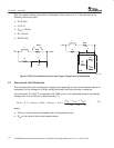
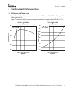
• To take full advantage of the ripple cancellation factor from interleaving, place the input
capacitors before the junction where the input voltage is distributed to each phase. Place the
output capacitors after the junction where all the inductors are connected;
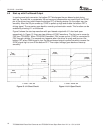
• Place the external drivers right next to the FETs and use at least 25 mil trace for gate drive
signal to improve noise immunity
• Place some ceramic capacitors in the input of each channel to filter the current spikes
• Place the NTC resistor right next to its related inductor for better thermal coupling
• 2 oz. or thicker copper is recommended to reduce the trace impedance
• Place enough vias along pads of the power components to increase thermal conduction
• Keep the current sensing traces as short as possible to avoid excessive noise pick up
• Place the output inductors as symmetric as possible in relation to the output connectors to
obtain similar voltage drop from the trace impedance