


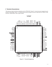
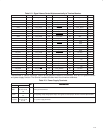
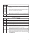

2–7
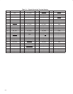
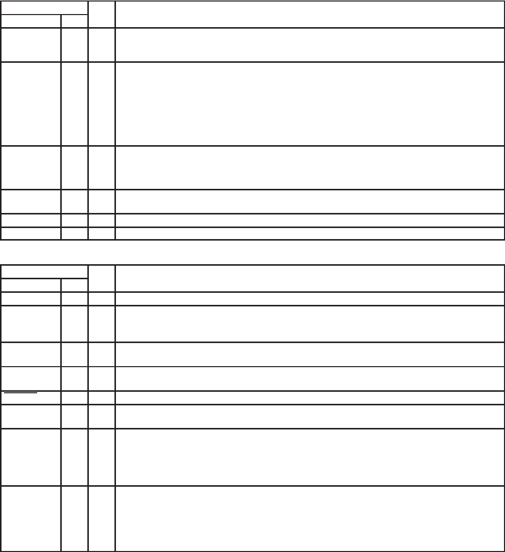
Table 2–7. IEEE 1394 PHY/Link Terminals
TERMINAL
I/O
DESCRIPTION
NAME NO.
I/O
DESCRIPTION
PHY_CTL1
PHY_CTL0
92
93
I/O
PHY-link interface control. These bidirectional signals control passage of information between the two devices.
The TSB12LV26 can only drive these terminals after the PHY has granted permission following a link request
(PHY_LREQ).
PHY_DATA7
PHY_DATA6
PHY_DATA5
PHY_DATA4
PHY_DATA3
PHY_DATA2
PHY_DATA1
PHY_DATA0
81
82
84
85
86
88
89
90
I/O
PHY-link interface data. These bidirectional signals pass data between the TSB12LV26 and the PHY device.
These terminals are driven by the TSB12LV26 on transmissions and are driven by the PHY on reception. Only
PHY_DATA1–PHY_DATA0 are valid for 100-Mbit speeds, PHY_DATA3–PHY_DATA0 are valid for 200-Mbit
speeds, and PHY_DATA7–PHY_DATA0 are valid for 400-Mbit speeds.
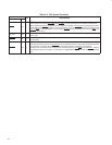
PHY_LINKON 98 I/O
LinkOn wake indication. The PHY_LINKON signal is pulsed by the PHY to activate the link, and 3.3-V signaling
is required.
When connected to the TSB41LV0X C/LKON terminal, a 1-kΩ series resistor is required between the link and
PHY.
PHY_LPS 99 I/O
Link power status. The PHY_LPS signal is asserted when the link is powered on, and 3.3-V signaling is
required.
PHY_LREQ 97 O Link request. This signal is driven by the TSB12LV26 to initiate a request for the PHY to perform some service.
PHY_SCLK 95 I System clock. This input from the PHY provides a 49.152-MHz clock signal for data synchronization.
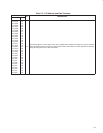
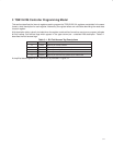
Table 2–8. Miscellaneous Terminals
TERMINAL
I/O
DESCRIPTION
NAME NO.
I/O
DESCRIPTION
CYCLEOUT 77 I/O This terminal provides an 8-kHz cycle timer synchronization signal.
CYCLEIN 78 I/O
The CYCLEIN terminal allows an external 8-kHz clock to be used as a cycle timer for synchronization with other
system devices.
If this terminal is not implemented, then it should be pulled high to the link V
CC
through a 4.7-kΩ resistor.
GPIO2 2 I/O
General-purpose I/O [2]. This terminal defaults as an input and if it is not implemented, then it is recommended
that it be pulled low to ground with a 220-Ω resistor.
GPIO3 3 I/O
General-purpose I/O [3]. This terminal defaults as an input and if it is not implemented, then it is recommended
that it be pulled low to ground with a 220-Ω resistor.
REG_EN 79 I Regulator enable. This terminal is pulled low to ground through a 220-Ω resistor.
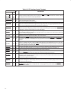
REG18
42
100
I
The REG18 terminals are connected to a 0.01 µF capacitor which, in turn, is connected to ground. The
capacitor provides a local bypass for the internal core voltage.
SCL 4 I/O
Serial clock. The TSB12LV26 determines whether a two-wire serial ROM is implemented at reset. If a two-wire
serial ROM is implemented, then this terminal provides the SCL serial clock signaling.
This terminal is implemented as open-drain, and for normal operation (a ROM is implemented in the design),
this terminal should be pulled high to the ROM V
CC
with a 2.7-kΩ resistor. Otherwise, it should be pulled low
to ground with a 220-Ω resistor.
SDA 5 I/O
Serial data. The TSB12LV26 determines whether a two-wire serial ROM is implemented at reset. If a two-wire
serial ROM is detected, then this terminal provides the SDA serial data signaling. This terminal must be wired
low to indicate no serial ROM is present.
This terminal is implemented as open-drain, and for normal operation (a ROM is implemented in the design),
this terminal should be pulled high to the ROM V
CC
with a 2.7-kΩ resistor. Otherwise, it should be pulled low
to ground with a 220-Ω resistor.