


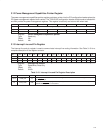


3–17
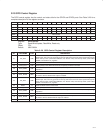
3.23 GPIO Control Register
The GPIO control register has the control and status bits for the GPIO2 and GPIO3 ports. See Table 3–20 for a
complete description of the register contents.
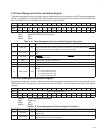
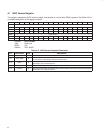
Bit 31 30 29 28 27 26 25 24 23 22 21 20 19 18 17 16
Name GPIO control
Type R/W R R/W R/W R R R RWU R/W R R/W R/W R R R RWU
Default 0 0 0 0 0 0 0 0 0 0 0 0 0 0 0 0
Bit 15 14 13 12 11 10 9 8 7 6 5 4 3 2 1 0
Name GPIO control
Type R R R R R R R R R R R R R R R R
Default 0 0 0 0 0 0 0 0 0 0 0 0 0 0 0 0
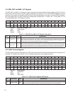
Register: GPIO control
Type: Read/Write/Update, ReadWrite, Read-only
Offset: FCh
Default: 0000 0000h
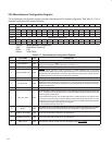
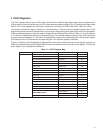
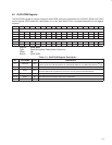
Table 3–20. GPIO Control Register Description
BIT FIELD NAME TYPE DESCRIPTION
31 INT_3EN R/W
When this bit is set, a TSB12LV26 general-purpose interrupt event occurs on a level change of the
GPIO3 input. This event may generate an interrupt, with mask and event status reported through the
OHCI interrupt mask (OHCI offset 88h/8Ch, see Section 4.22) and interrupt event (OHCI offset
80h/84h, see Section 4.21) registers.
30 RSVD R Reserved. Bit 30 returns 0 when read.
29 GPIO_INV3 R/W GPIO3 polarity invert. When this bit is set, the polarity of GPIO3 is inverted.
28 GPIO_ENB3 R/W
GPIO3 enable control. When this bit is set, the output is enabled. Otherwise, the output is high
impedance.
27–25 RSVD R Reserved. Bits 27–25 return 0s when read.
24 GPIO_DATA3 RWU
GPIO3 data. Reads from this bit return the logical value of the input to GPIO3. Writes to this bit update
the value to drive to GPIO3 when output is enabled.
23 INT_2EN R/W
When this bit is set, a TSB12LV26 general-purpose interrupt event occurs on a level change of the
GPIO2 input. This event may generate an interrupt, with mask and event status reported through the
OHCI interrupt mask (OHCI offset 88h/8Ch, see Section 4.22) and interrupt event (OHCI offset
80h/84h, see Section 4.21) registers.
22 RSVD R Reserved. Bit 22 returns 0 when read.
21 GPIO_INV2 R/W GPIO2 polarity invert. When this bit is set, the polarity of GPIO2 is inverted.
20 GPIO_ENB2 R/W
GPIO2 enable control. When this bit is set, the output is enabled. Otherwise, the output is high
impedance.
19–17 RSVD R Reserved. Bits 19–17 return 0s when read.
16 GPIO_DATA2 RWU
GPIO2 data. Reads from this bit return the logical value of the input to GPIO2. Writes to this bit update
the value to drive to GPIO2 when the output is enabled.
15–0 RSVD R Reserved. Bits 15–0 return 0s when read.