


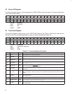
3–6
3.6 Class Code and Revision ID Register
The class code and revision ID register categorizes the TSB12LV26 as a serial bus controller (0Ch), controlling an
IEEE 1394 bus (00h), with an OHCI programming model (10h). Furthermore, the TI chip revision is indicated in the
least significant byte. See Table 3–5 for a complete description of the register contents.
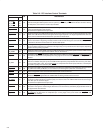
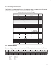
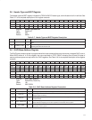
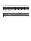
Bit 31 30 29 28 27 26 25 24 23 22 21 20 19 18 17 16
Name Class code and revision ID
Type R R R R R R R R R R R R R R R R
Default 0 0 0 0 1 1 0 0 0 0 0 0 0 0 0 0
Bit 15 14 13 12 11 10 9 8 7 6 5 4 3 2 1 0
Name Class code and revision ID
Type R R R R R R R R R R R R R R R R
Default 0 0 0 1 0 0 0 0 0 0 0 0 0 0 0 0
Register: Class code and revision ID
Type: Read-only
Offset: 08h
Default: 0C00 1000h
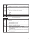
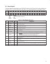
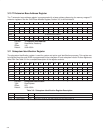
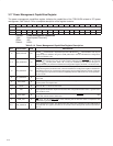
Table 3–5. Class Code and Revision ID Register Description
BIT FIELD NAME TYPE DESCRIPTION
31–24 BASECLASS R
Base class. This field returns 0Ch when read, which broadly classifies the function as a serial bus
controller.
23–16 SUBCLASS R
Subclass. This field returns 00h when read, which specifically classifies the function as controlling an
IEEE 1394 serial bus.
15–8 PGMIF R
Programming interface. This field returns 10h when read, indicating that the programming model is
compliant with the
1394 Open Host Controller Interface Specification
.
7–0 CHIPREV R Silicon revision. This field returns 00h when read, indicating the silicon revision of the TSB12LV26.
3.7 Latency Timer and Class Cache Line Size Register
The latency timer and class cache line size register is programmed by host BIOS to indicate system cache line size
and the latency timer associated with the TSB12LV26. See Table 3–6 for a complete description of the register
contents.
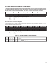
Bit 15 14 13 12 11 10 9 8 7 6 5 4 3 2 1 0
Name Latency timer and class cache line size
Type R/W R/W R/W R/W R/W R/W R/W R/W R/W R/W R/W R/W R/W R/W R/W R/W
Default 0 0 0 0 0 0 0 0 0 0 0 0 0 0 0 0
Register: Latency timer and class cache line size
Type: Read/Write,
Offset: 0Ch
Default: 0000h
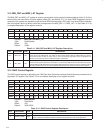
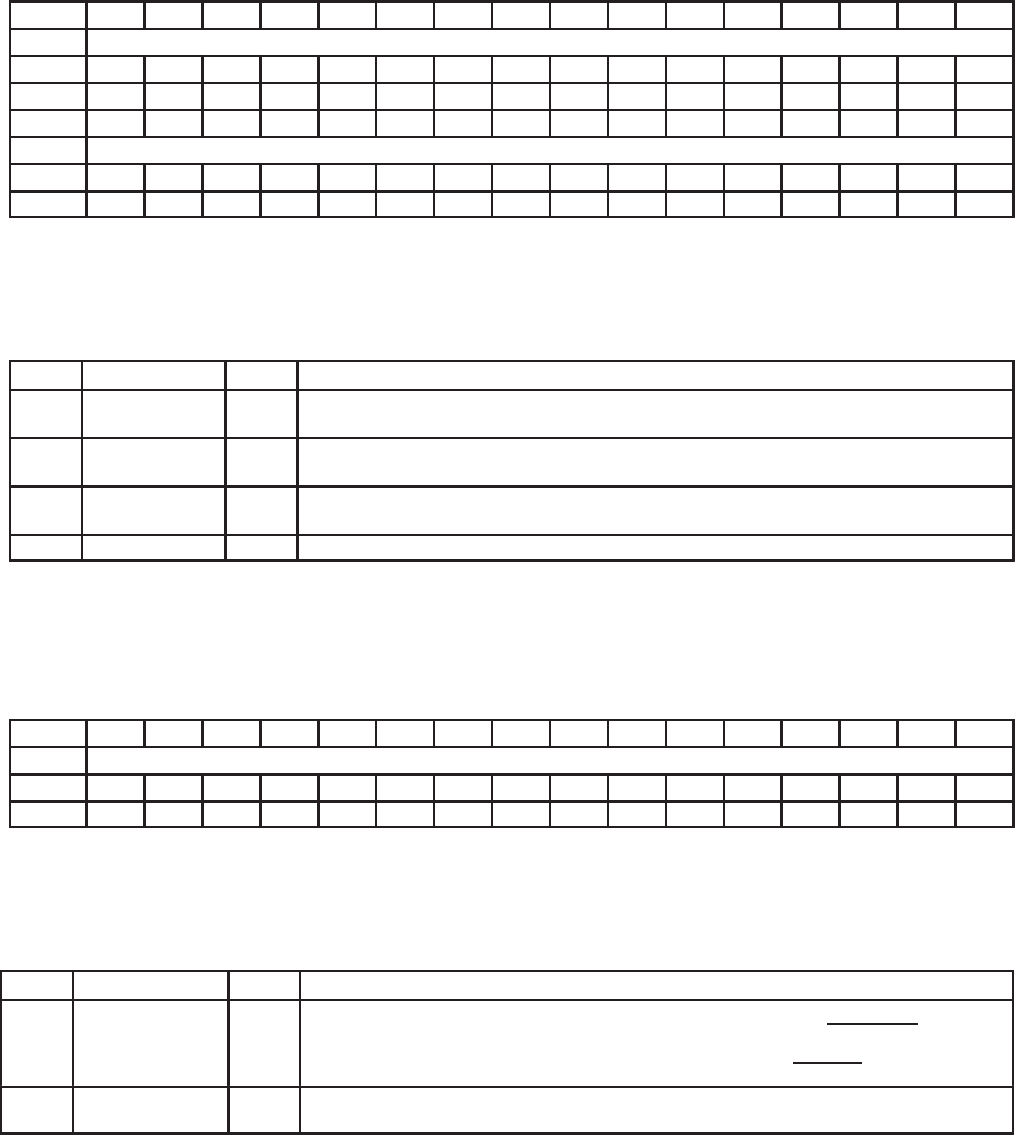
Table 3–6. Latency Timer and Class Cache Line Size Register Description
BIT FIELD NAME TYPE DESCRIPTION
15–8 LATENCY_TIMER R/W
PCI latency timer. The value in this register specifies the latency timer for the TSB12LV26, in units of
PCI clock cycles. When the TSB12LV26 is a PCI bus initiator and asserts PCI_FRAME
, the latency
timer begins counting from zero. If the latency timer expires before the TSB12LV26 transaction has
terminated, then the TSB12LV26 terminates the transaction when its PCI_GNT
is deasserted.
7–0 CACHELINE_SZ R/W
Cache line size. This value is used by the TSB12LV26 during memory write and invalidate, memory
read line, and memory read multiple transactions.