


© 2003 - 2008 TOSHIBA TEC CORPORATION All rights reserved GD-1150/1151/1200/1201/1160/1260
ELECTRICAL CIRCUITS
4 - 7
4
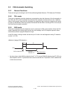
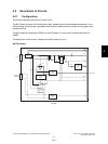
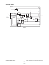
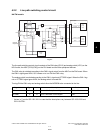
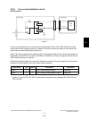
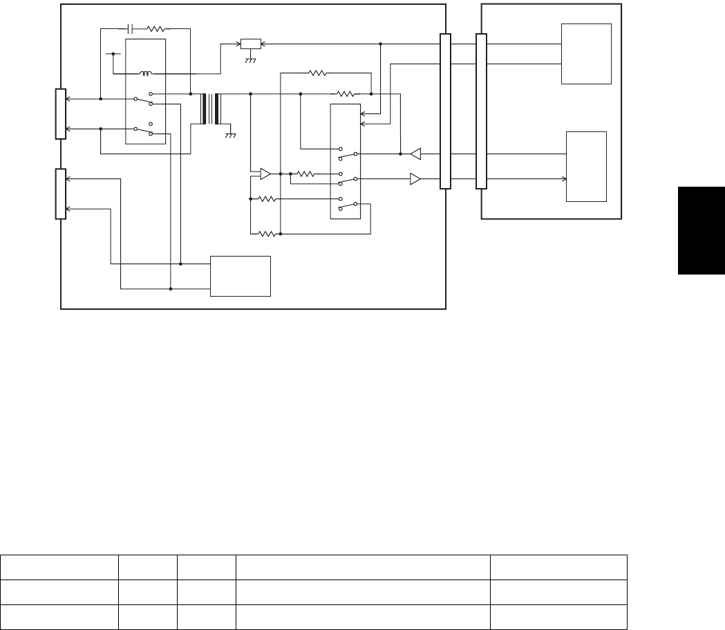
4.2.2 Line path switching control circuit
NA/TW models
Fig. 4-7
The line path switching control circuit consists of the CML relay (RLY2) and analog switch (IC51) on the
NCU board, the ASIC (IC29 [IC26]) on the FAX board and the other peripheral devices.
The CML relay is switched according to the CML1 signal output from the ASIC on the FAX board. When
the CML1 signal goes HIGH, Q51 comes on to turn ON the CML relay.
The analog switch is switched according to the CML1 signal and ATT3DB1 signal. When the CML1 sig-
nal or ATT3DB1 signal goes HIGH, the analog switch is turned ON.
Turning ON the CML relay and analog switch allow the MODEM to be connected to the line.
* Values in [ ] are for GD-1151/1201 in case that the descriptions vary between GD-1150/1200 and
GD-1151/1201.
Signal Name Type Active Description Destination
CML1 O H Line 1 CML Relay Control Signal RLY2, IC51
ATT3DB1 O H Line 1 Attenuator Control Signal IC51
C5 R4
NCU board
CN10CN11
4
3
Line
External
telephone
3
4
Lb
La
a2
b2
+12V
RLY2
CML relay
AG
T1
AG
0
1
0
1
3
10
8
121
9
4
Q51
Ring signal
detection
circuit
IC53
R59
R66
3
1
2
5
7
6
13
0
1
0
1
0
1
14
15
4
10
9,11
R71
IC51
Analog
switch
3
112
672
6
IC52
IC53
CN9
CN501
6
3
2
1
FAX board
CML1
ATT3DB1
TXOUT1
RXIN1
22
21
IC29
[
IC26
]
ASIC
32
28,29
IC12
[
IC9
]
MODEM
R68
R67
08/03