


VXI Technology, Inc.
42 SM8000 Series Programming
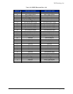
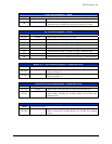
NVM Access Register – Read
ADDR
Plug-In LA+0x20
D15-D1 Unused All Bits are always 1.
D0
Reads back the serial data stream from the selected SMIP II board.
Note that only one SMIP II board may be read back at a time.
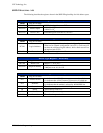
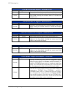
NVM Access Register – Write
ADDR
Plug-In LA+0x20
D15-D7 Unused Data written to these bits have no effect.
D6 Serial clock for module 5; should be a logic 1 when not used.
D5 Serial clock for module 4; should be a logic 1 when not used.
D4 Serial clock for module 3; should be a logic 1 when not used.
D3 Serial clock for module 2; should be a logic 1 when not used.
D2 Serial clock for module 1; should be a logic 1 when not used.
D1 Serial clock for module 0; should be a logic 1 when not used.
D0 Serial data input for all modules; must be a logic 1 when not used.
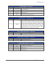
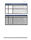
Board X, Y Used Address Register – Read and Write
ADDR
Plug-In LA+0x22 to 0x26
D15-D8
Sets the actual number of words of address space used by the
relays on board's X.
D7-D0
Sets the actual number of words of address space used by the
relays on board's Y.
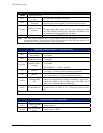
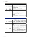
Trace RAM Start High Register – Read and Write
ADDR
Plug-In LA+0x28
D15-D4 Unused Data written to these bits have no affect and read back as 1s.
D3-D0
Sets the four most significant bits of the starting address of the
Trace RAM, allowing the available RAM to be divided into
multiple traces.
Trace RAM Start Low Register – Read and Write
ADDR
Plug-In LA+0x2A
D15-D0
Sets the 16 least significant bits of the starting address of the Trace
RAM, allowing the available RAM to be divided into multiple
traces.