


44 Register-Based Programming
Appendix B
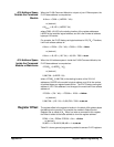
Reset and Registers When the E1470A undergoes power-on or a *RST in SCPI, the bits of the
registers are put into the following states. Manufacturer ID Register, Device
Type Register, and Status/Control Register are unaffected and Relay
Control Registers have a “0” written to each bit. This forces all relays to
their power-on/reset state. To reset the module, write a “1” and then a “0”
to bit 0 of the Status/Control Register.
Register Definitions
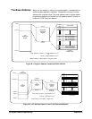
You can program the E1470A Cascade RF Switch module using its
hardware registers. The procedures for reading or writing to a register
depend on your operating system and programming language. Whatever
the access method, you will need to identify each register with its address.
These addresses are given in Table B-2.
The interrupt protocol supported is “release on interrupt acknowledge.”
An interrupt is cleared by a VXIbus interrupt acknowledge cycle.
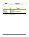
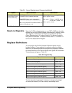
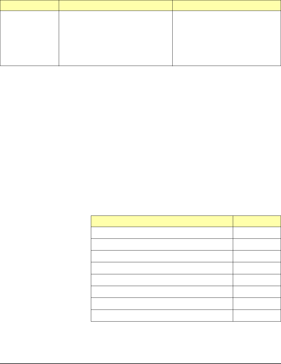
Table B-1. General Register-based Programming Method
System Typical Commands Base Address
External Computer
(over GPIB to E1406
Command Module)
VXI:READ? logical_address, offset
VXI:WRITE logical_address,offset,data
DIAG:PEEK? (Base_addr + offset,width)
DIAG:POKE (Base_addr +offset,width, data)
When using DIAG:PEEK? and DIAG:POKE, the
width must be either 8 or 16.
Module Logical Address setting (LADDR*)
offset = register number
Base_addr = 1FC000
h
+ (LADDR * 40)
h
or
= 2,080,768 + (LADDR * 64)
offset = register number
* LADDR = E1470 Logical Address = 120 / 8 = 15
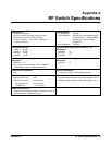
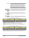
Table B-2. Register Map
Register Name Address
Manufacturer ID (read only register) Base + 00
h
Device ID (read only register) Base + 02
h
Card /Status/Control (read/write register) Base + 04
h
Relay Control Register (read/write register) Base + 20
h
Relay Control Register (read/write register) Base + 22
h
Relay Control Register (read/write register) Base + 24
h
Relay Control Register (read/write register) Base + 26
h
Relay Control Register (read/write register) Base + 28
h