


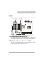
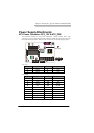

Albatron Anniversary Special Edition PX845PEV-800
28
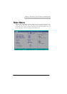
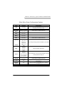
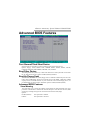
Advanced Chipset Features
DRAM Timing Selectable
This item determines DRAM clock/ timing using SPD or manual configuration. Make sure
your memory module has SPD (Serial Presence Data), if you want to select the <By SPD>
option. Options: Manual, By SPD (default).
CAS Latency Time
This item determines CAS Latency. When synchronous DRAM is installed, the number of
clock cycles of CAS latency depends on the DRAM timing. Do not reset this field from the
default value specified by the system designer. Options: 1.5,2,2.5 and By SPD (default).
Active to Precharge Delay
This item allows you to select DRAM Active to Precharge Delay. Options: 7, 6, 5, By SPD
(default).
DRAM RAS# to CAS# Delay
This item allows you to select a delay time between the CAS and RAS strobe signals. It only
applies when DRAM is written to, read from, or refreshed. Options: 3,2 and default is by SPD.
DRAM RAS# Precharge
This item allows you to select the DRAM RAS# precharge time. The ROW address strobe
must precharge again before DRAM is refreshed. An inadequate configuration may result in
incomplete data. Options: 3,2 and By SPD (default).
Refresh Mode Select
Select the refresh mode. Options: 15.6 us, 7.8 us, 64 us, Auto (default).
System BIOS Cacheable
When enabled, accesses to system BIOS ROM addressed at F0000H-FFFFFH are cached,
provided that the cache controller is enabled. Options: Enabled (default), Disabled.
Video BIOS Cacheable
Select “Enabled” to allow caching of the video BIOS which may improve performance. If any
other program writes to this memory area, a system error may result. Options: Enabled,
Disabled (default).
Memory Hole at 15M-16M
When enabled, you can reserve an area of system memory for ISA adapter ROM. When this
area is reserved, it cannot be cached. Refer to the user documentation of the peripheral you are
installing for more information. Options: Disabled (default), Enabled.
Delayed Transaction
The chipset has an embedded 32-bit posted write buffer to support delay transaction cycles.
Select “Enabled” to support compliance with PCI specifications. Options: Disabled, Enabled
(default).
Delay Prior to Thermal
Select the delay time before thermal activation from high temperatures.
Options: 4 Min, 8 Min, 16 Min (default), 32 Min.