


P
R
E
L
I
M
I
N
A
R
Y
T
E
C
H
N
I
C
A
L
D
A
T
A
a
Preliminary Technical Data
DSP
Microcomputer
This information applies to a product under development. Its characteristics
and specifications are subject to change without notice. Analog Devices
assumes no obligation regarding future manufacturing unless otherwise
agreed to in writing.
One Technology Way, P.O.Box 9106, Norwood, MA 02062-9106, U.S.A.
Tel:781/329-4700 World Wide Web Site: http://www.analog.com
Fax:781/326-8703 ©Analog Devices,Inc., 2000
REV. PrA
ADSP-2192
ADSP-2192 DUAL-CORE DSP FEATURES
320 MIP Dual ADSP-219x DSP in a 144-lead LQFP
package with PCI, USB, Sub-ISA, and CardBus
Interfaces
3.3V/5V PCI 2.2 Compliant 33MHz / 32-bit Interface with
Bus Mastering over four DMA Channels with
Scatter-Gather Support
Integrated USB 1.1 Compliant Interface
AC ‘97 serial interface supports external modem,
handset, and audio codecs
Dual 160 MIPS ADSP-219x DSPs with 140K Words of
Memory and 4K x 16-bit Shared Data Memory
DSP P0 Memory Includes: 64K x 16-bit Data Memory,
16K x 24-bit Program Memory, and Boot ROM
DSP P1 Memory Includes: 32K x 16-bit Data Memory,
16K x 24-bit Program Memory, and Boot ROM
ADSP-219X DSP CORE FEATURES
6.25 ns Instruction Cycle Time (Internal), for up to 160
MIPS Sustained Performance
ADSP-218x Family Code Compatible with the Same
Easy to Use Algebraic Syntax
Single-cycle Instruction Execution
Dual Purpose Program Memory for Both Instruction and
Data Storage
Fully Transparent Instruction Cache Allows Dual
Operand Fetches in Every Instruction Cycle
Unified Memory Space Permits Flexible Address
Generation, Using Two Independent DAG Units
Independent ALU, Multiplier/Accumulator, and Barrel
Shifter Computational Units with Dual 40-bit
Accumulators
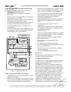
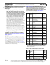
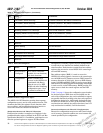
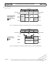
Figure 1. ADSP-2192 Dual-Core DSP Block Diagram
INTERRUPT CONTROLLER/
TIMER/FLAGS
CACHE
64 X 24-BIT
PM ADDRESS BUS
DM ADDRESS BUS
PM DATA BUS
DM DATA BUS
24
16
ADSP-219X
DSP CORE
DATA
REGISTER
FILE
MULT
BARREL
SHIFTER
ALU
INPUT
REGISTERS
RESULT
REGISTERS
16 X 16-BIT
CORE
INTERFACE
24
24
BUS
CONNECT
(PX)
PROGRAM
SEQUENCER
DAG1
4X4X16
DAG2
4X4X16
INTERRUPT CONTROLLER/
TIMER/FLAGS
CACHE
64 X 24-BIT
PM ADDRESS BUS
DM ADDRESS BUS
PM DATA BUS
DM DATA BUS
24
16
ADSP-219X
DSP CORE
DATA
REGISTER
FILE
MULT
BARREL
SHIFTER
ALU
INPUT
REGISTERS
RESULT
REGISTERS
16 X 16-BIT
CORE
INTERFACE
24
24
BUS
CONNECT
(PX)
PROGRAM
SEQUENCER
DAG1
4X4X16
DAG2
4X4X16
PROCESSOR P0 PROCESSOR P1
SHARED
MEMORY
4K؋
؋؋
؋16 DM
ADDR DATA
P0
MEMORY
16K؋
؋؋
؋24 PM
64K
؋
؋؋
؋
16 DM
BOOT ROM
P1
MEMORY
16K؋
؋؋
؋24 PM
32K
؋
؋؋
؋
16 DM
BOOT ROM
ADDR DATA ADDR DATA
P0 DMA
CONTROLLER
FIFOS
SHARED DSP
I/O MAPPED
REGISTERS
P1 DMA
CONTROLLER
FIFOS
ADDR DATA
HOST PORT
PCI 2.2
OR
USB 1.1
SERIAL PORT
AC'97
COMPLIANT
GP I/O PINS
(& OPTIONAL
SERIAL
EEPROM)
JTAG
EMULATION
PORT
ADDR DATAADDR DATA