


P
R
E
L
I
M
I
N
A
R
Y
T
E
C
H
N
I
C
A
L
D
A
T
A
P
R
E
L
I
M
I
N
A
R
Y
T
E
C
H
N
I
C
A
L
D
A
T
A
For current information contact Analog Devices at (781) 461-3881
ADSP-2192 October 2000
This information applies to a product under development. Its characteristics and specifications are subject to change with-
out notice. Analog Devices assumes no obligation regarding future manufacturing unless otherwise agreed to in writing.
12 REV. PrA
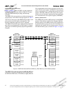
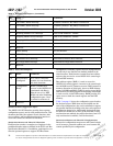
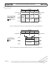
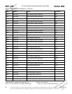
ADSP-2192 PCI Memory Map
The ADSP-2192 On-Chip Memory is mapped to the PCI
Address Space. Because some ADSP-2192 Memory Blocks
are 24-bits wide (Program Memory) while others are
16-bits (Data Memory), two different footprints are avail-
able in PCI Address Space. These footprints are available to
each PCI function by accessing different PCI Base Address
Registers (BAR).
BAR2 supports 24-bit “Unpacked” Memory Access. BAR3
supports 16-bit “Packed” Memory Access.
In 24-bit (BAR2) Mode, each 32 bits (4 Consecutive PCI
Byte Address Locations, which make up one PCI Data
word) correspond to a single ADSP-2192 Memory Loca-
tion. BAR2 Mode is typically used for Program Memory
Access. Byte3 is always unused. Bytes[2:0] are used for
24-bit Memory Locations. Bytes[2:1] are used for 16-bit
Memory Locations as shown in the example figure.
In 16-bit (BAR3) Mode, each 32-bit (4 Consecutive PCI
Byte Address Locations) PCI Data word corresponds to
two ADSP-2192 Memory Locations. Bytes[3:2] contain
one 16-bit Data Word, Bytes[1:0] contain a second 16-bit
Data Word. BAR3 Mode is typically used for Data Memory
Access. Only the 16 MSBs of a Data Word are accessed in
24-bit Blocks; the 8 LSBs are ignored.
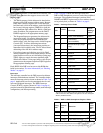
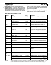
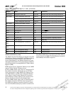
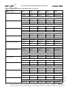
0x2D- 0x2C Subsystem Vendor ID 0x11D4 Writable from the DSP during initialization
0x2F- 0x2E Config 0 Subsystem Device ID 0x2192 Writable from the DSP during initialization
Config 1 Subsystem Device ID 0x219A Writable from the DSP during initialization
Config 2 Subsystem Device ID 0x219E Writable from the DSP during initialization
0x33- 0x30 Expansion ROM Base Address 0x0 Unimplemented
0x34 Capabilities Pointer 0x40 Read-only
0x3C Interrupt Line 0x0
0x3D Interrupt Pin 0x1 Uses INTA
Pin
0x3E Min_Gnt 0x1 Read-only
0x3F Max_Lat 0x4 Read-only
0x40 Capability ID 0x1 Power Management Capability Identifier
0x41 Next_Cap_Ptr 0x0 Read-only
0x43-
0x42
Power Management Capabilities 0x6C22 Writable from the DSP during initialization
0x45-
0x44
Power Management Control/Status 0x0 Bits 15 and 8 initialized only on Power-up
0x46 Power Management Bridge 0x0 Unimplemented
0x47 Power Management Data 0x0 Unimplemented
Table 7. PCI Configuration Space 0, 1, and 2 (Continued)
Address Name Reset Comments