


P
R
E
L
I
M
I
N
A
R
Y
T
E
C
H
N
I
C
A
L
D
A
T
A
P
R
E
L
I
M
I
N
A
R
Y
T
E
C
H
N
I
C
A
L
D
A
T
A
This information applies to a product under development. Its characteristics and specifications are subject to change with-
out notice. Analog Devices assumes no obligation regarding future manufacturing unless otherwise agreed to in writing.
5REV. PrA
For current information contact Analog Devices at (781) 461-3881
ADSP-2192October 2000
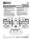
mechanisms to generate a 24-bit address for each bus. The
DSP has three functions that support access to the full
memory map.
• The DAGs generate 24-bit addresses for data fetches
from the entire DSP memory address range. Because
DAG index (address) registers are 16 bits wide and
hold the lower 16-bits of the address, each of the DAGs
has its own 8-bit page register (DMPGx) to hold the
most significant eight address bits. Before a DAG gen-
erates an address, the program must set the DAG’s
DMPGx register to the appropriate memory page.
• The Program Sequencer generates the addresses for
instruction fetches. For relative addressing instruc-
tions, the program sequencer bases addresses for
relative jumps, calls, and loops on the 24-bit Program
Counter (PC). In direct addressing instructions
(two-word instructions), the instruction provides an
immediate 24-bit address value. The PC allows linear
addressing of the full 24 bit address range.
• For indirect jumps and calls that use a 16-bit DAG
address register for part of the branch address, the Pro-
gram Sequencer relies on an 8-bit Indirect Jump page
(IJPG) register to supply the most significant eight
address bits. Before a cross page jump or call, the pro-
gram must set the program sequencer’s IJPG register to
the appropriate memory page.
Each ADSP-219x DSP core has an on-chip ROM that
holds boot routines. For more information, see “Booting
Modes” on page 31.
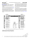
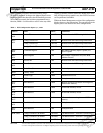
Interrupts
The interrupt controller lets the DSP respond to thirteen
interrupts with minimum overhead. The controller imple-
ments an interrupt priority scheme as shown in Table 1 on
page 5. Applications can use the unassigned slots for soft-
ware and peripheral interrupts. The DSP’s Interrupt
Control (ICNTL) register (shown in Table 3 on page 6)
provides controls for global interrupt enable, stack interrupt
configuration, and interrupt nesting.
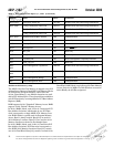
Table 2 on page 5 shows the interrupt vector and
DSP-to-DSP semaphores at reset of each of the peripheral
interrupts. The peripheral interrupt’s position in the
IMASK and IRPTL register and its vector address depend
on its priority level, as shown in Table 1 on page 5.
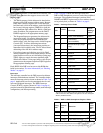
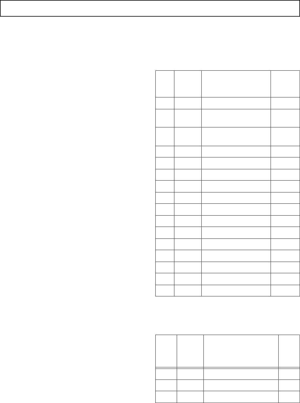
Table 1. Interrupt Vector Table
Bit
Priorit
y
Interrupt
Vector
Address
Offset
1
1
The interrupt vector address values are represented as offsets from
address 0x01 0000. This address corresponds to the start of Program
Memory in DSP P0 and P1.
0 1 Reset (non-maskable) 0x00
12 Powerdown
(non-maskable)
0x04
2 3 Kernel interrupt (single
step)
0x08
3 4 Stack Status 0x0C
45 Mailbox 0x10
56 Timer 0x14
6 7 Reserved 0x18
7 8 PCI Bus Master 0x1C
8 9 DSP-DSP 0x20
9 10 FIFO0 Transmit 0x24
10 11 FIFO0 Receive 0x28
11 12 FIFO1 Transmit 0x2C
12 13 FIFO1 Receive 0x30
13 14 Reserved 0x34
14 15 Reserved 0x38
15 16 AC’97 Frame 0x3C
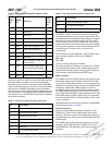
Table 2. DSP-to-DSP Semaphores Register Table
Flag
Bit
Direct-
ion
Function
DSP
Core
Flag
In
0 Output DSP-DSP Semaphore 0
1 Output DSP-DSP Semaphore 1
2 Output DSP-DSP Interrupt