


P
R
E
L
I
M
I
N
A
R
Y
T
E
C
H
N
I
C
A
L
D
A
T
A
P
R
E
L
I
M
I
N
A
R
Y
T
E
C
H
N
I
C
A
L
D
A
T
A
This information applies to a product under development. Its characteristics and specifications are subject to change with-
out notice. Analog Devices assumes no obligation regarding future manufacturing unless otherwise agreed to in writing.
29REV. PrA
For current information contact Analog Devices at (781) 461-3881
ADSP-2192October 2000
An active low RST input (to be derived from PCI RST and
possible other sources) and an active-high IRQ interrupt
output are available. Power Management is handled by the
ADSP-2192 inputs PDW1–0
/PME_EN and the
ADSP-2192 output PMERQ
. PDW1–0 should be the
inversion of the PCI power state in the function’s PMCSR
register. PDW1
is connected to AD21, and PDW0 is con-
nected to AD20
.
Assertion of PDW1
low signals a power-down interrupt to
the DSP.
Deassertion of PDW1
high causes a wake-up of the DSP.
The PME_EN output from the Combo Master should
reflect the current PCI function PME_EN bit and should
be connected to the ADSP-2192 AD20 pin. The PMI_EN
bit should be set to enable interrupt and wake-up of the
DSP upon any change of the PME_EN state. If PME_EN
is turned off, the DSPs can wake up if necessary and then
power themselves and the ADSP-2192 completely down
(clocks stopped).
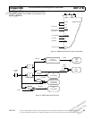
PCI Interface to DSP Memory
The PCI interface can directly access the DSP memory
space using DMA transfers. The transactions can be either
slave transfers, in which the host initiates the transaction, or
master transfers, in which the ADSP-2192 initiates the PCI
transaction. The registers that control PCI DMA transfers
are accessible from both the DSP (on the Peripheral Device
Control Bus) and the PCI Bus.
The PCI/Sub-ISA Bus uses the Peripheral Device Control
Register Space which is distributed throughout the
ADSP-2192 and connected through the Peripheral Device
Control Bus. The PCI bus can access these registers
directly.
USB Interface to DSP Memory
The USB interface can directly access the DSP memory
space using DMA transfers to memory locations specified
by the USB endpoints. The registers that control USB end-
point DMA transfers are accessible from both the DSP (on
the Peripheral Device Control Bus) and the USB Bus.
The Peripheral Device Control Register Space is distrib-
uted throughout the ADSP-2192 and connected through
the Peripheral Device Control Bus. The USB Bus can
access these registers directly.
AC’97 Codec Interface to DSP Memory
Transfers from AC’97 data to DSP memory are accom-
plished using DMA transfer through the DSP FIFOs. Each
DSP has four FIFOs available for data transfers to/from the
AC’97 Codec Interface. The registers that control FIFO
DMA transfers are only accessible from within the DSP and
are defined as part of the core register space.
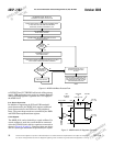
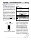
Data FIFO Architecture
Each DSP core within the ADSP-2192 contains four FIFOs
which provide a data communication path to the rest of the
chip. Two of the FIFOs are input FIFOs, receiving data into
the DSP. The other two FIFOs are transmit FIFOs, sending
data from the DSP to the codec, AC'97 interface, or the
other DSP. Each FIFO is eight words deep and sixteen bits
wide. Interrupts to the DSP can be generated when some
words have been received in the input FIFOs, or when some
words are empty in the Transmit FIFOs.
The interface to the FIFOs on the DSP is simply a register
interface to the Peripheral Interface bus. TX0, RX0, TX1,
and RX1 are the primary FIFO registers in the universal
register map of the DSP. The FIFOs can be used to gener-
ate interrupts to the DSP based upon FIFO transactions or
can initiate DMA requests.
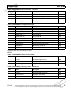
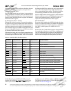
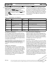
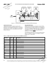
Table 24. Sub-ISA Indirect Access Registers
ISAA[3:1] Name Reset Comments
0x0 Control Register Address 0x0000 Address and direction control for registers accesses
0x1 Reserved
0x2 Control Register Data 0x0000 Data for register accesses
0x3 Reserved
0x5-0x4 DSP Memory Address 0x000000 Address and direction control for DSP memory
accesses
0x7-0x6 DSP Memory Data 0x000000 Data for DSP memory accesses.