


P
R
E
L
I
M
I
N
A
R
Y
T
E
C
H
N
I
C
A
L
D
A
T
A
P
R
E
L
I
M
I
N
A
R
Y
T
E
C
H
N
I
C
A
L
D
A
T
A
For current information contact Analog Devices at (781) 461-3881
ADSP-2192 October 2000
This information applies to a product under development. Its characteristics and specifications are subject to change with-
out notice. Analog Devices assumes no obligation regarding future manufacturing unless otherwise agreed to in writing.
10 REV. PrA
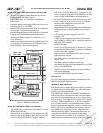
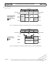
ADSP-2192 PCI Configuration Space
The ADSP-2192 PCI Interface provides three separate
configuration spaces, one for each possible function. This
document describes the registers in each function, their
reset condition, and how the three functions interact to
access and control the ADSP-2192 hardware.
Similarities Between the Three PCI Functions
Each function contains a complete set of registers in the
predefined header region as defined in the PCI Local Bus
Specification Revision 2.2. In addition, each function con-
tains the optional registers to support PCI Bus Power
Management. Generally, registers that are unimplemented
or read-only in one function are similarly defined in the
other functions. Each function contains four base address
registers that are used to access ADSP-2192 control regis-
ters and DSP memory.
Base address register (BAR) 1 is used to access the
ADSP-2192 control registers. Accesses to the control regis-
ters via BAR1 uses PCI memory accesses. BAR1 requests a
memory allocation of 1024 bytes. Access to DSP memory
occurs via BAR2 and BAR3. BAR2 is used to access 24-bit
DSP memory (for DSP program downloading) while BAR3
is used to access 16-bit DSP memory. BAR4 provides I/O
space access to both the control registers and the DSP
memory.
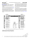
Table 7 on page 11 shows the configuration space headers
for the three spaces. While these are the default uses for
each of the configurations, they can be redefined to support
any possible function by writing to the class code register of
that function during boot. Additionally, during boot time,
the DSP can disable one or more of the functions. If only
two functions are enabled, they will be functions 0 and 1. If
only one function is enabled, it will be function 0.
Interactions Between the Three PCI Configurations
Because the configurations must access and control a single
set of resources, potential conflicts can occur between the
control specified by the configuration.
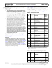
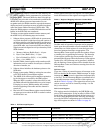
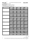
3 Tx0 DMA Channel Interrupt Transmit Channel 0 Bus Master Transactions
4 Tx1 DMA Channel Interrupt Transmit Channel 1 Bus Master Transactions
5 Incoming Mailbox 0 PCI Interrupt PCI to DSP Mailbox 0 Transfer
6 Incoming Mailbox 1 PCI Interrupt PCI to DSP Mailbox 1 Transfer
7 Outgoing Mailbox 0 PCI Interrupt DSP to PCI Mailbox 0 Transfer
8 Outgoing Mailbox 1 PCI Interrupt DSP to PCI Mailbox 1 Transfer
9 Reserved
10 Reserved
11 GPIO Wakeup I/O Pin Initiated
12 AC’97 Wakeup AC’97 Interface Initiated
13 PCI Master Abort Interrupt PCI Interface Master Abort Detected
14 PCI Target Abort Interrupt PCI Interface Target Abort Detected
15 Reserved
Table 5. PCI Interrupt Register (Continued)
Bit Name Comments
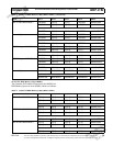
Table 6. PCI Control Register
Bit Name Comments
1-0 PCI Functions
Configured
00 = one PCI Function
enabled, 01= two functions,
10= three functions
2Configuration
Ready
When 0, disables PCI
accesses to the ADSP-2192
(terminated with Retry).
Must be set to 1 by DSP
ROM code after initializing
configuration space. Once
1, cannot be written to 0.
15-3 Reserved