


P
R
E
L
I
M
I
N
A
R
Y
T
E
C
H
N
I
C
A
L
D
A
T
A
P
R
E
L
I
M
I
N
A
R
Y
T
E
C
H
N
I
C
A
L
D
A
T
A
This information applies to a product under development. Its characteristics and specifications are subject to change with-
out notice. Analog Devices assumes no obligation regarding future manufacturing unless otherwise agreed to in writing.
17REV. PrA
For current information contact Analog Devices at (781) 461-3881
ADSP-2192October 2000
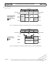
16-bit PCI DSP I/O Memory Map (BAR4)
PCI Base Address Register (BAR 4) allows indirect access
to the ADSP-2192 Control Registers and DSP Memory.
The DSP Memory Indirect Access Registers accessible
from BAR4 are as follows:
DSP P0 Memory Indirect Address Space occupies PCI
BAR4 Space 0x000000 -> 0x01FFFF
DSP P1 Memory Indirect Address Space occupies PCI
BAR4 Space 0x020000 -> 0x03FFFF
All Indirect DSP Memory Accesses are 24-bit or 16-bit
Word Accesses.
Using the USB Interface
The ADSP-2192 USB design enables the ADSP-2192 to be
configured and attached to a single device with multiple
interfaces and various endpoint configurations, as follows:
1. Programmable descriptors and a class-specific com-
mand interpreter are accessible through the USB 8052
registers. An 8052-compatible MCU is supported
on-board, to enable soft downloading of different con-
figurations, and support of standard or class-specific
commands.
2. A total of 8 user-defined endpoints are provided. End-
points can be configured as BULK, ISO, or INT, and
can be grouped
USB DSP Register Definitions
For each endpoint, four registers are defined to provide a
memory buffer in the DSP. These registers are defined for
each endpoint shared by all defined interfaces, for a total of
4x8 = 32 registers. These registers are read/write by the
DSP only.
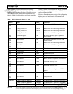
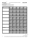
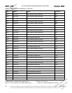
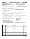
Table 10. 16-bit PCI DSP I/O Space Indirect Access Registers Map (BAR 4 Mode)
Offset Name Reset Comments
0x03-0x00 Control Register Address 0x0000 Address and direction control for registers accesses
0x07-0x04 Control Register Data 0x0000 Data for register accesses
0x0B-0x08 DSP Memory Address 0x000000 Address and Direction control for Indirect DSP
memory accesses
0x0F-0x0C DSP Memory Data 0x000000 Data for DSP memory accesses
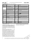
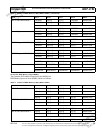
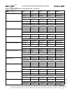
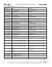
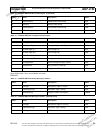
Table 11. USB DSP Register Definitions
Page Address Name Comment
0x0C 0x0-0x3 DSP Memory Buffer Base Addr EP4
0x0C 0x4-0x5 DSP Memory Buffer Size EP4
0x0C 0x6-0x7 DSP Memory Buffer RD Offset EP4
0x0C 0x8-0x9 DSP Memory Buffer WR Offset EP4
0x0C 0x10-0x13 DSP Memory Buffer Base Addr EP5
0x0C 0x14-0x15 DSP Memory Buffer Size EP5
0x0C 0x16-0x17 DSP Memory Buffer RD Offset EP5