


P
R
E
L
I
M
I
N
A
R
Y
T
E
C
H
N
I
C
A
L
D
A
T
A
P
R
E
L
I
M
I
N
A
R
Y
T
E
C
H
N
I
C
A
L
D
A
T
A
For current information contact Analog Devices at (781) 461-3881
ADSP-2192 October 2000
This information applies to a product under development. Its characteristics and specifications are subject to change with-
out notice. Analog Devices assumes no obligation regarding future manufacturing unless otherwise agreed to in writing.
28 REV. PrA
If for some reason the host sends more data than the max-
packetsize, the USB core accepts it, as long as there is
sufficient room in the FIFO.
Since the DSP controls the read pointer, it must perform a
similar calculation to determine if there is sufficient data in
the FIFO to begin processing. Once it has consumed some
amount of data, the DSP will need to update the Memory
Buffer Read Offset register.
IN Transactions (Host <- Device)
When an IN transaction arrives for a particular endpoint,
the USB core once again computes how much read data is
available in the FIFO. It also determines if the amount of
read data is greater than or equal to the maxpacketsize. If
both conditions are met, the USB core will transfer the data.
Upon receiving ACK from the host, the USB core updates
the Memory Buffer Read Offset register.
If the amount of read data is less than the maxpacketsize (a
short packet), the USB core determines whether to send the
data based upon a NAK count limit. This is a 4-bit field in
the Endpoint Stall Policy register that can be programmed
with a value indicating how many NAK's should be sent
prior to transmitting a short packet. This allows flexibility
in determining how IRPs are retired via short packets.
Since the DSP controls the write pointer, it must determine
if there is sufficient room in the FIFO for placing new data.
Once it has completed writes to the FIFO, it needs to
update the Memory Buffer Write Offset register.
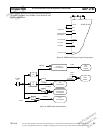
Sub-ISA Interface
In systems which combine the ADSP-2192 chip with other
devices on a single PCI interface, the ADSP-2192 Sub-ISA
mode is used to provide a simpler interface (to a PCI func-
tion ASIC), which bypasses the ADSP-2192’s PCI
interface.
In this mode, the Combo Master assumes all responsibility
for interfacing the function to the PCI bus, including provi-
sion of Configuration Space registers for the ADSP-2192
system as a separate PnP function. In Sub-ISA Mode the
PCI Pins are reconfigured for ISA operation, as follows.
In Sub-ISA mode, the ADSP-2192’s PCI protocol is
replaced with an ISA-like, asynchronous protocol con-
trolled by the strobes IOR
, IOW and AEN. Access is
possible only to the PCI Base Address 4 (BAR4) Registers
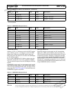
(the InDirect Access Registers). The Sub-ISA Address Map
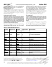
is shown in Table 23 on page 28.
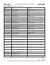
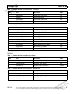
Table 23. Sub-ISA (PCI) Pin Descriptions
Pin Name PCI Direction
1
ISA Alias ISA Direction ISA Description.
AD[15:0] In/Out ISAD[15:0] In/Out Data
AD[18:16] In/Out ISAA[3:1] In Register Address
AD[31:22] In/Out Unused In Tie to GND in Sub-ISA Mode
RST
In RST In Reset
CBE0
In/Out IOW In Write Strobe
CBE1
In/Out IOR In Read Strobe
CBE2
In/Out AEN In Chip Select (Access Enable)
INTA
Out (o/d) IRQ Out (CMOS) Interrupt (Active High)
AD21 In/Out PDW1
In PCI D-state MSB (inverted) Power-Down
AD20 In/Out PDW0
In PCI D-state LSB (inverted) Power-Down
AD19 In/Out PME_EN In PME Enable
PME
Out (o/d) PMERQ Out (o/d) Power Management Event
CLK In Unused In Tie to GND in Sub-ISA Mode
CLKRUN
In/Out IOCHRDY Out IO Ready
CLKRUN Out IOCHRDY Out Acknowledge
1
o/d = Open Drain