


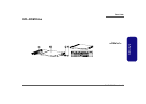
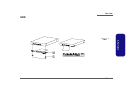

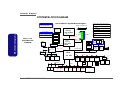
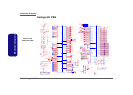
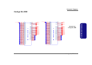
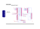
Schematic Diagrams
B-1
B.Schematic Diagrams
Appendix B:Schematic Diagrams
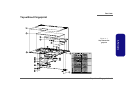
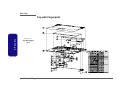
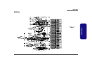
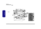
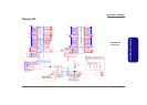
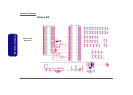
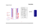
This appendix has circuit diagrams of the M860TU notebook’s PCB’s. The following table indicates where to find the
appropriate schematic diagram.
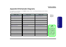
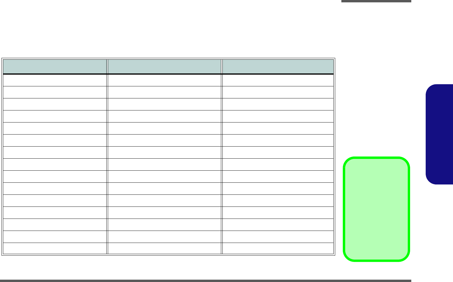
Diagram - Page Diagram - Page Diagram - Page
SYSTEM BLOCK DIAGRAM - Page B - 2 ICH9-M 4/4, Power - Page B - 17 Power 1.5V/0.75V - Page B - 32
Penryn 1/2 - Page B - 3 ODD, USB2.0 & eSATA - Page B - 18 Power 3.3VM/1.8VS/1.05VM - Page B - 33
Penryn 2/2 - Page B - 4 Clock Generator - Page B - 19 Power 3VS/5VS / Power S/W - Page B - 34
Cantiga 1/6, Host - Page B - 5 PCI-E LAN RTL8111C, RJ45RJ11 - Page B - 20 Power VDD3/VDD5/3.3V/5V - Page B - 35
Cantiga 2/6, PEG - Page B - 6 Card Reader & 1394 JMB380 - Page B - 21 Power VCORE - Page B - 36
Cantiga 3/6, DDR - Page B - 7 New Card, CCD, Fan - Page B - 22 Mini Card/WLAN - Page B - 37
Cantiga 4/6, Power 1 - Page B - 8 KBC-ITE IT8512 - Page B - 23 MXM PCI-E Type III - Page B - 38
Cantiga 5/6, GND - Page B - 9 HDMI, 3G - Page B - 24 Board to Board CON/TPM - Page B - 39
Cantiga 6/6, Power 2 - Page B - 10 LED, Screw Hole - Page B - 25 Button Board - Page B - 40
DDR3 SO-DIMM 1 - Page B - 11 Azalia CODEC ALC662 - Page B - 26 Click Board - Page B - 41
DDR3 SO-DIMM 2 - Page B - 12 Audio AMP - Page B - 27 Finger Printer Board - Page B - 42
LCD - Page B - 13 SRS, MDC, BT - Page B - 28 SIM Card Board - Page B - 43
ICH9-M 1/4, SATA - Page B - 14 DVI, INV - Page B - 29
ICH9-M 2/4, PCI, USB - Page B - 15 Power Charger, DC-In - Page B - 30
ICH9-M 3/4 - Page B - 16 Power GPU - Page B - 31
Table B - 1
Schematic
Diagrams
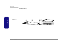
Version Note
The schematic dia-
grams in this chapter
are based upon ver-
sion 6-7P-M8605-003.
If your mainboard (or
other boards) are a lat-
er version, please
check with the Service
Center for updated di-
agrams (if required).