


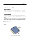
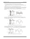
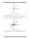
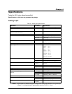

-10V
+10V
Input Voltage
0
16383
Output Code
8192
Figure 3-10. Ideal ADC transfer function
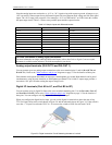
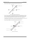
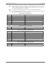
The offset error is measured at mid-scale. Ideally, a zero volt input should produce an output code of 8192. Any
deviation from this is an offset error.
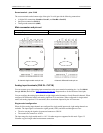
Figure 3-11
Figure 3-11. ADC transfer function with offset error
shows an example of a UMDAS 0802DA transfer function with a ±2.44 mV offset error. Offset error
affects all codes equally by shifting the entire transfer function up or down along the input voltage axis.
The accuracy plots in Figure 3-11 are drawn for clarity and are not drawn to scale.
-10V
+10V
Input Voltage
0
16383
Offset=2.44mV
Ideal
Actual
Output Code
2.44mV
8192
Gain error is a change in the slope of the transfer function from the ideal, and is typically expressed as a
percentage of full-scale. Gain error is easily converted to voltage by multiplying the full-scale (FS) input by the
error.
3-9
UMDAS 0802DA User's Guide Functional Details