


CY7C0850AV, CY7C0851AV
CY7C0852AV, CY7C0853AV
Document #: 38-06070 Rev. *H Page 25 of 32
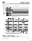
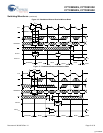
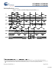
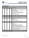
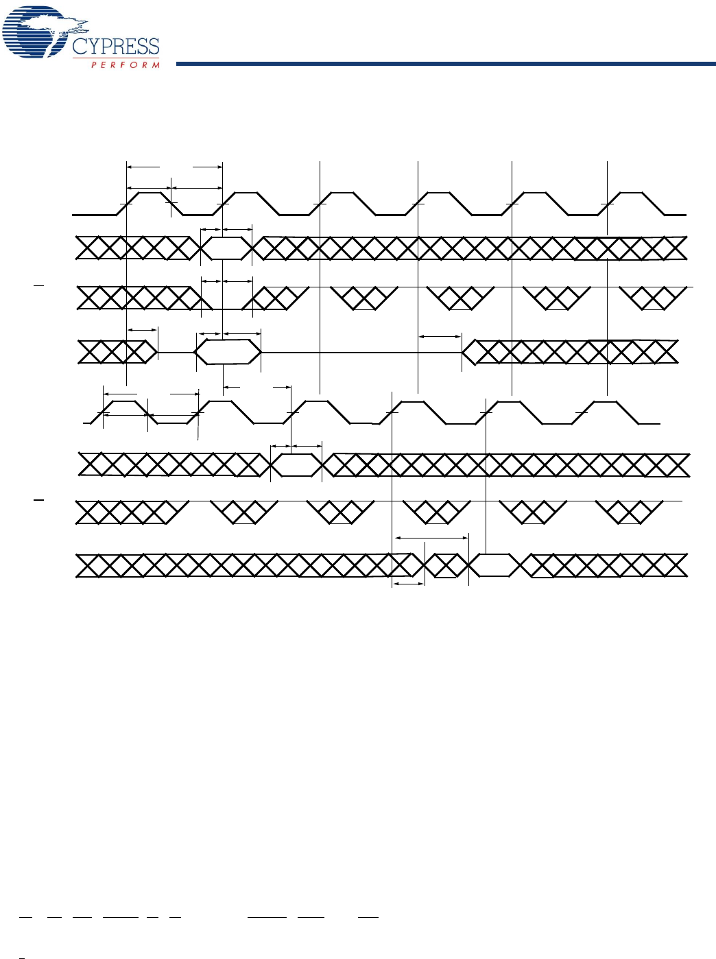
Figure 21. Left_Port (L_Port) Write to Right_Port (R_Port) Read
[39, 40, 41]
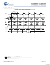
Switching Waveforms (continued)
t
SA
t
HA
t
SW
t
HW
t
CH2
t
CL2
t
CYC2
CLK
L
R/W
L
A
n
D
n
t
CKHZ
t
HD
t
SA
A
n
t
HA
Q
n
t
DC
t
CCS
t
SD
t
CKLZ
t
CH2
t
CL2
t
CYC2
t
CD2
L_PORT
ADDRESS
L_PORT
DATA
IN
CLK
R
R/W
R
R_PORT
ADDRESS
R_PORT
DATA
OUT
Notes
39.CE
0
= OE = ADS = CNTEN = B0 – B3 = LOW; CE
1
= CNTRST = MRST = CNT/MSK = HIGH.
40.This timing is valid when one port is writing, and other port is reading the same location at the same time. If t
CCS
is violated, indeterminate data is Read out.
41.If t
CCS
< minimum specified value, then R_Port is Read the most recent data (written by L_Port) only (2 * t
CYC2
+ t
CD2
) after the rising edge of R_Port's clock. If t
CCS
>
minimum specified value, then R_Port is Read the most recent data (written by L_Port) (t
CYC2
+ t
CD2
) after the rising edge of R_Port's clock.
[+] Feedback