


CY7C0850AV, CY7C0851AV
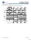
CY7C0852AV, CY7C0853AV
Document #: 38-06070 Rev. *H Page 27 of 32
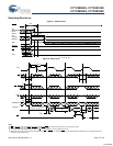
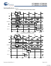
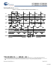
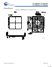
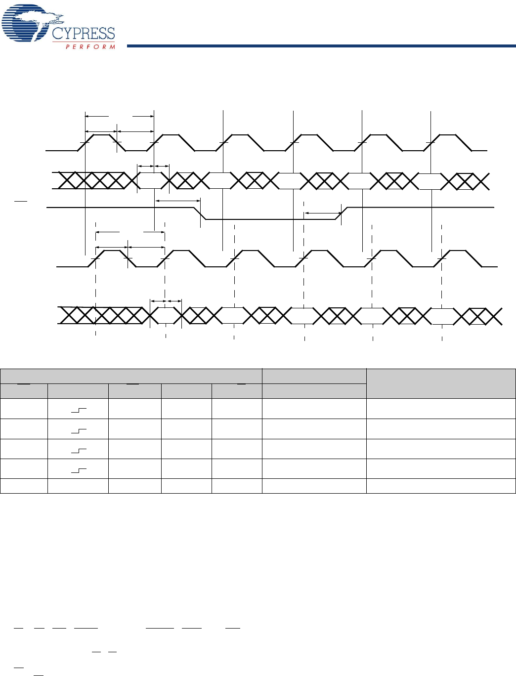
Figure 23. MailBox Interrupt Timing
[46, 47, 48, 49, 50]
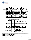
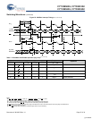
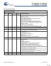
Table 7. Read/Write and Enable Operation
(Any Port)
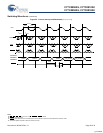
[1, 8, 51, 52]
Inputs Outputs
Operation
OE CLK CE
0
CE
1
R/W DQ
0
– DQ
35
X H X X High-Z Deselected
X X L X High-Z Deselected
XLHLD
IN
Write
LLHHD
OUT
Read
H X L H X High-Z Outputs Disabled
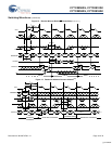
Switching Waveforms (continued)
t
CH2
t
CL2
t
CYC2
CLK
L
t
CH2
t
CL2
t
CYC2
CLK
R
3FFFF
t
SA
t
HA
A
n+3
A
n
A
n+1
A
n+2
L_PORT
ADDRESS
A
m
A
m+4
A
m+1
3FFFF
A
m+3
R_PORT
ADDRESS
INT
R
t
SA
t
HA
t
SINT
t
RINT
Notes
46.CE
0
= OE = ADS = CNTEN = LOW; CE
1
= CNTRST = MRST = CNT/MSK = HIGH.
47.Address “3FFFF” is the mailbox location for R_Port of a 9M device.
48.L_Port is configured for Write operation, and R_Port is configured for Read operation.
49.At least one byte enable (B0
– B3) is required to be active during interrupt operations.
50.Interrupt flag is set with respect to the rising edge of the Write clock, and is reset with respect to the rising edge of the Read clock.
51.OE
is an asynchronous input signal.
52.When CE
changes state, deselection and Read happen after one cycle of latency.
[+] Feedback