CY7C601xx, CY7C602xx
Document 38-16016 Rev. *E Page 15 of 68
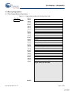
11.2 Data Memory Organization
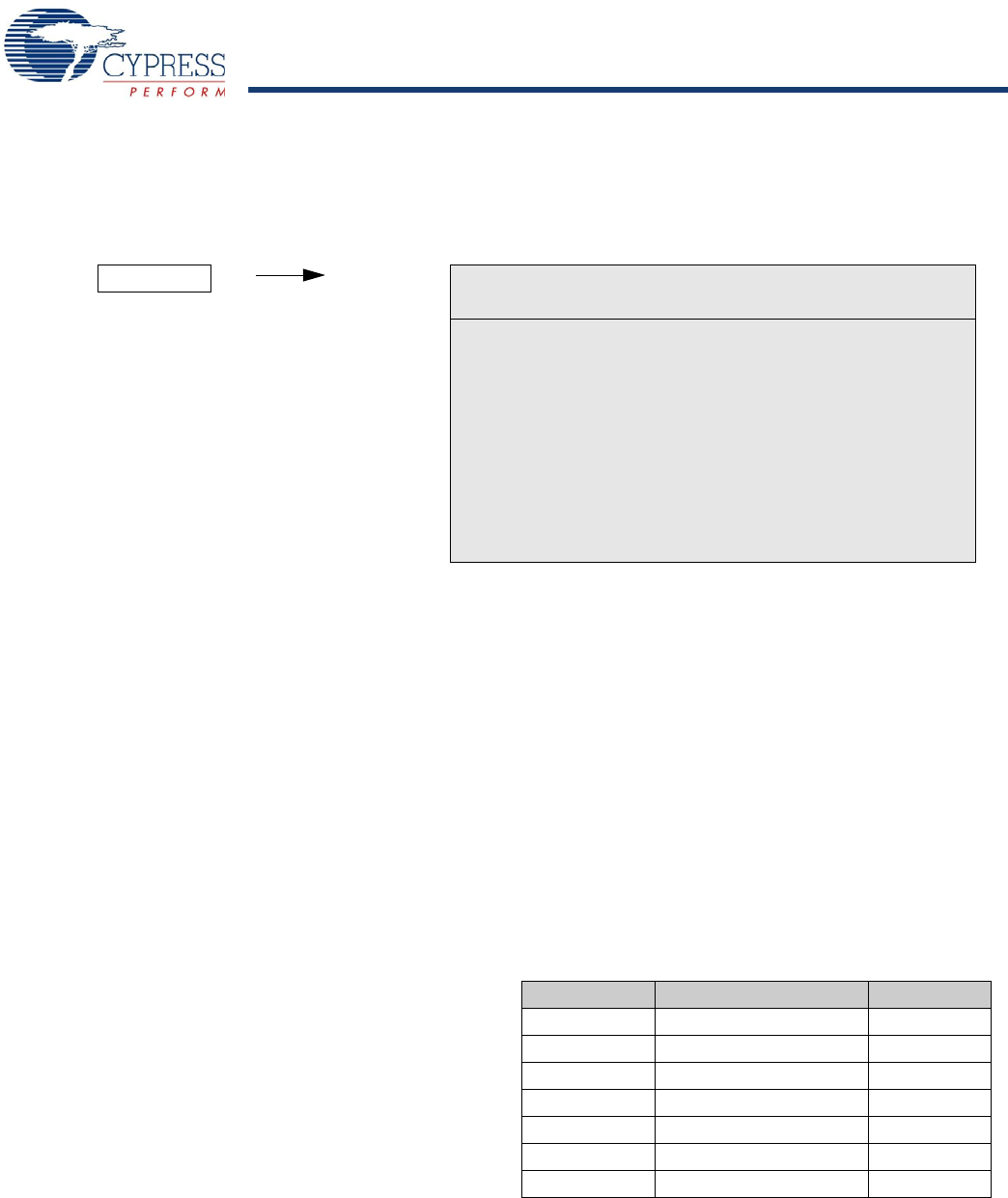
The CY7C601xx and CY7C602xx microcontrollers provide up to 256 bytes of data RAM
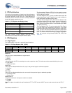
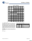
Figure 11-2. Data Memory Organization
11.3 Flash
This section describes the Flash block of enCoRe II LV. Much of
the visible Flash functionality, including programming and
security, are implemented in the M8C Supervisory Read Only
Memory (SROM). enCoRe II LV Flash has an endurance of 1000
erase and write cycles and a ten year data retention capability.
11.3.1 Flash Programming and Security
All Flash programming is performed by code in the SROM. The
registers that control Flash programming are only visible to the
M8C CPU when it is executing out of SROM. This makes it
impossible to read, write, or erase the Flash by avoiding the
security mechanisms implemented in the SROM.
Customer firmware only programs Flash via SROM calls. The
data or code images are sourced through any interface with the
appropriate support firmware. This type of programming requires
a ‘boot-loader’—a piece of firmware resident on the Flash. For
safety reasons this boot-loader is not overwritten during firmware
rewrites.
The Flash provides four extra auxiliary rows to hold Flash block
protection flags, boot time calibration values, configuration
tables, and any device values. The routines to access these
auxiliary rows are documented in the SROM section. The
auxiliary rows are not affected by the device erase function.
11.3.2 In-System Programming
enCoRe II LV devices enable in-system programming by using
the P1.0 and P1.1 pins as the serial programming mode
interface. This allows an external controller to make the enCoRe
II LV part enter serial programming mode and then use the test
queue to issue Flash access functions in the SROM.
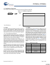
11.4 SROM
The SROM holds the code to boot the part, calibrate circuitry, and
perform Flash operations (Table 11-1 lists the SROM functions).
The functions of the SROM are accessed in normal user code or
operating from Flash. The SROM exists in a separate memory
space from user code. To access SROM functions, the Super-
visory System Call instruction (SSC) is executed, which has an
opcode of 00h. Before executing SSC, the M8C’s accumulator is
loaded with the desired SROM function code from Table 11-1.
Undefined functions causes a HALT if called from user code. The
SROM functions execute code with calls; therefore, the functions
require stack space. With the exception of Reset, all of the
SROM functions have a parameter block in SRAM that must be
configured before executing the SSC. Table 11-2 lists all possible
parameter block variables. The meaning of each parameter, with
regards to a specific SROM function, is described later in this
section.
After Reset Address
8-bit PSP 0x00 Stack begins here and grows upward
Top of RAM Memory 0xFF
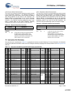
Table 11-1. SROM Function Codes
Function Code Function Name Stack Space
00h SWBootReset 0
01h ReadBlock 7
02h WriteBlock 10
03h EraseBlock 9
05h EraseAll 11
06h TableRead 3
07h CheckSum 3
[+] Feedback [+] Feedback


