CY7C601xx, CY7C602xx
Document 38-16016 Rev. *E Page 32 of 68
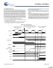
14.1 Sleep Sequence
The SLEEP bit is an input into the sleep logic circuit. This circuit
is designed to sequence the device into and out of the hardware
sleep state. The hardware sequence to put the device to sleep
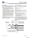
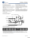
is shown in Figure 14-1. and is defined as follows.
1. Firmware sets the SLEEP bit in the CPU_SCR0 register. The
Bus Request (BRQ) signal to the CPU is immediately
asserted. This is a request by the system to halt CPU
operation at an instruction boundary. The CPU samples BRQ
on the positive edge of CPUCLK.
2. Due to the specific timing of the register write, the CPU issues
a Bus Request Acknowledge (BRA) on the following positive
edge of the CPU clock. The sleep logic waits for the following
negative edge of the CPU clock and then asserts a system
wide Power Down (PD) signal. In Figure 14-1. the CPU is
halted and the system wide power down signal is asserted.
3. The system wide PD signal controls several major circuit
blocks: the Flash memory module, the internal 24 MHz
oscillator, the EFTB filter, and the bandgap voltage reference.
These circuits transition into a zero power state. The only
operational circuits on chip are the low power oscillator, the
bandgap refresh circuit, and the supply voltage monitor
(POR/LVD) circuit.
The external crystal oscillator on enCoRe II LV devices is not
automatically powered down when the CPU enters the sleep
state. Firmware must explicitly disable the external crystal oscil-
lator to reduce power to levels specified.
14.1.1 Low Power in Sleep Mode
To achieve the lowest possible power consumption during
suspend or sleep, the following conditions are observed in
addition to considerations for the sleep timer and external crystal
oscillator:
■
All GPIOs are set to outputs and driven low
■
Clear P11CR[0], P10CR[0]
■
Set P10CR[1]
■
Make sure 32 KHz oscillator clock is not selected as clock
source to ITMRCLK, TCAPCLK, and not even as clock output
source onto P01_CLKOUT pin.
All the other blocks go to the power down mode automatically on
suspend.
The following steps are user configurable and help in reducing
the average suspend mode power consumption.
1. Configure the power supply monitor at a large regular
intervals, control register bits are 1,EB[7:6] (power system
sleep duty cycle PSSDC[1:0]).
2. Configure the low power oscillator into low power mode,
control register bit is LOPSCTR[7].
For low power considerations during sleep when external clock
is used as the CPUCLK source, the clock source must be held
low to avoid unintentional leakage current. If the clock is held
high, then there may be a leakage through M8C. To avoid current
consumption make sure ITMRCLK and TCPCLK are not sourced
by either low power 32 KHz oscillator or 24 MHz crystal-less
oscillator. Do not select 24 MHz or 32 KHz oscillator clocks on to
the P01_CLKOUT pin.
Figure 14-1. Sleep Timing
Firmware write to SCR
SLEEP bit causes an
immediate BRQ
IOW
SLEEP
BRQ
PD
BRA
CPUCLK
CPU captures BRQ
on next CPUCLK
edge
CPU
responds with
a BRA
On the falling edge of CPUCLK,
PD is asserted. The 24/48 MHz
system clock is halted; the Flash
and bandgap are powered down
[+] Feedback [+] Feedback


