CY7C601xx, CY7C602xx
Document 38-16016 Rev. *E Page 58 of 68
19.4.3 Interrupt Vector Clear Register
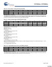
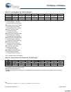
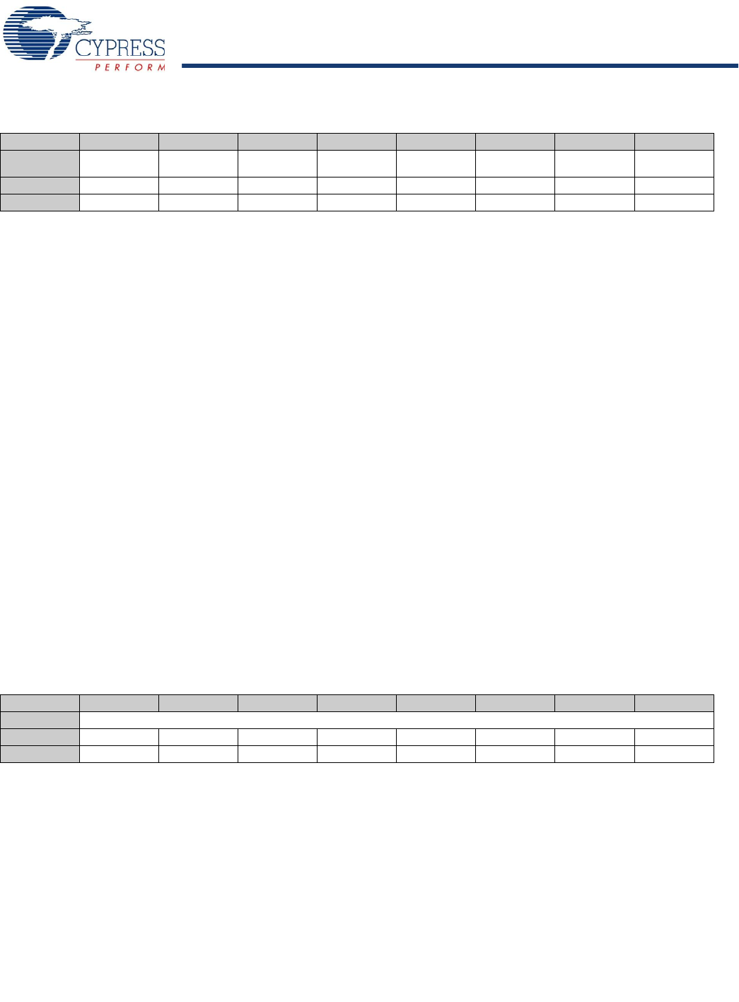
Table 19-8. Interrupt Mask 0 (INT_MSK0) [0xE0] [R/W]
Bit # 7 6 5 4 3 2 1 0
Field GPIO Port 1
Int Enable
Sleep Timer
Int Enable
INT1
Int Enable
GPIO Port 0
Int Enable
SPI Receive
Int Enable
SPI Transmit
Int Enable
INT0
Int Enable
POR/LVD
Int Enable
Read/Write R/W R/W R/W R/W R/W R/W R/W R/W
Default 0 0 0 0 000 0
Bit 7: GPIO Port 1 Interrupt Enable
0 = Mask GPIO Port 1 interrupt
1 = Unmask GPIO Port 1 interrupt
Bit 6: Sleep Timer Interrupt Enable
0 = Mask Sleep Timer interrupt
1 = Unmask Sleep Timer interrupt
Bit 5: INT1 Interrupt Enable
0 = Mask INT1 interrupt
1 = Unmask INT1 interrupt
Bit 4: GPIO Port 0 Interrupt Enable
0 = Mask GPIO Port 0 interrupt
1 = Unmask GPIO Port 0 interrupt
Bit 3: SPI Receive Interrupt Enable
0 = Mask SPI Receive interrupt
1 = Unmask SPI Receive interrupt
Bit 2: SPI Transmit Enable
0 = Mask SPI Transmit interrupt
1 = Unmask SPI Transmit interrupt
Bit 1: INT0 Interrupt Enable
0 = Mask INT0 interrupt
1 = Unmask INT0 interrupt
Bit 0: POR/LVD Interrupt Enable
0 = Mask POR/LVD interrupt
1 = Unmask POR/LVD interrupt
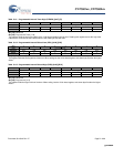
Table 19-9. Interrupt Vector Clear Register (INT_VC) [0xE2] [R/W]
Bit # 7 6 5 4 3 2 1 0
Field Pending Interrupt [7:0]
Read/Write R/W R/W R/W R/W R/W R/W R/W R/W
Default 0 0 0 0 000 0
The Interrupt Vector Clear Register (INT_VC) holds the interrupt vector for the highest priority pending interrupt when read, and
when written clears all pending interrupts.
Bit [7:0]: Pending Interrupt [7:0]
8-bit data value holds the interrupt vector for the highest priority pending interrupt. Writing to this register clears all pending
interrupts.
Note
4. Available only on CY7C601xx
P2.7, P3.7, P0.0, P0.1; CY7C602xx P1.3,P1.4,P1.5,P1.6,P1.7.
[+] Feedback [+] Feedback


