


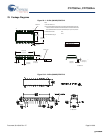
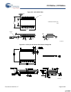
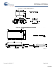
CY7C601xx, CY7C602xx
Document 38-16016 Rev. *E Page 59 of 68
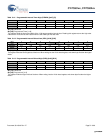
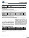
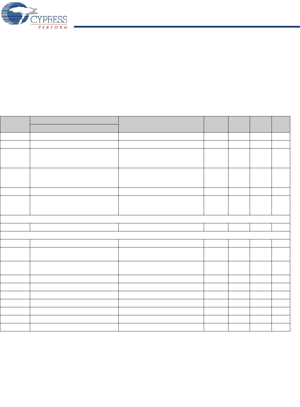
20. Absolute Maximum Ratings
Storage Temperature ................................... –40°C to +90°C
Ambient Temperature with Power Applied..... –0°C to +70°C
Supply Voltage on V
CC
Relative to V
SS
..........–0.5V to +7.0V
DC Input Voltage ............................... –0.5V to + V
CC
+ 0.5V
DC Voltage Applied to Outputs in
High-Z State....................................... –0.5V to + V
CC
+ 0.5V
Maximum Total Sink Output Current into Port 0
and 1 and Pins............................................................. 70 mA
Maximum Total Source Output Current into GPIO Pins30 mA
Maximum On-chip Power Dissipation
on any GPIO Pin......................................................... 50 mW
Power Dissipation ....................................................300 mW
Static Discharge Voltage .............................................2200V
Latch-up Current ...................................................... 200 mA
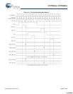
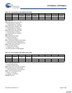
20.1 DC Characteristics
Parameter
Description
Conditions Min Typical Max Unit
General
V
CC1
Operating Voltage CPU speed <= 12 MHz 2.7 3.6 V
T
FP
Operating Temperature Flash programming 0 70 °C
I
CC1
V
CC
Operating Supply Current CPU =12 MHz, Vdd = 3.3V, T = 75C
CPU =12 MHz, Vdd = 2.7V, T = 25C
4.25
3.25
11
-
mA
mA
I
CC2
V
CC
Operating Supply Current CPU = 6 MHz, Vdd = 3.3V, T = 75C
CPU = 6 MHz, Vdd = 3.3V, T = 25C
3.15
2.45
9
-
mA
mA
I
CC3
V
CC
Operating Supply Current CPU = 3 MHz, Vdd = 2.7V, T = 25C 2.0 - mA
I
SB1
Standby Current Internal and external oscillators,
Bandgap, Flash, CPU clock, timer
clock all disabled
10 μA
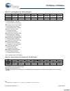
Low Voltage Detect
V
LVD
Low Voltage Detect Trip Voltage LVDCR [2:0] set to 000 2.681 2.7 V
General Purpose IO Interface
R
UP
Pull Up Resistance 4 12 KΩ
V
ICR
Input Threshold Voltage Low, CMOS
Mode
Low to high edge 40% 65% V
CC
V
ICF
Input Threshold Voltage Low, CMOS
Mode
High to low edge 30% 55% V
CC
V
HC
Input Hysteresis Voltage, CMOS Mode High to low edge 3% 10% V
CC
V
ILTTL
Input Low Voltage, TTL Mode 0.72 V
V
IHTTL
Input HIGH Voltage, TTL Mode 1.6 V
V
OL1
Output Low Voltage, High Drive
[4]
I
OL1
= 50 mA 1.4 V
V
OL2
Output Low Voltage, High Drive
[4]
I
OL1
= 25 mA 0.4 V
V
OL3
Output Low Voltage, Low Drive I
OL2
= 8 mA 0.8 V
V
OH
Output High Voltage
[4]
I
OH
= 2 mA V
CC
– 0.5 V
Notes
5. Refer to Clocking on page 21 for details on loading proper trim values.
6. In Master mode first bit is available 0.5 SPICLK cycle before Master clock edge available on the SCLK pin.
[+] Feedback [+] Feedback