CY7C601xx, CY7C602xx
Document 38-16016 Rev. *E Page 33 of 68
14.2 Wakeup Sequence
When asleep, the only event that wakes the system up is an
interrupt. The global interrupt enable of the CPU flag register
need not be set. Any unmasked interrupt wakes the system up.
It is optional for the CPU to actually take the interrupt after the
wakeup sequence. The wakeup sequence is synchronized to the
32 kHz clock for purposes of sequencing a startup delay, to allow
the Flash memory module enough time to power up before the
CPU asserts the first read access. Another reason for the delay
is to allow the oscillator, Bandgap, and LVD and POR circuits
time to settle before actually being used in the system. As shown
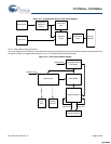
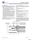
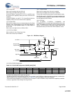
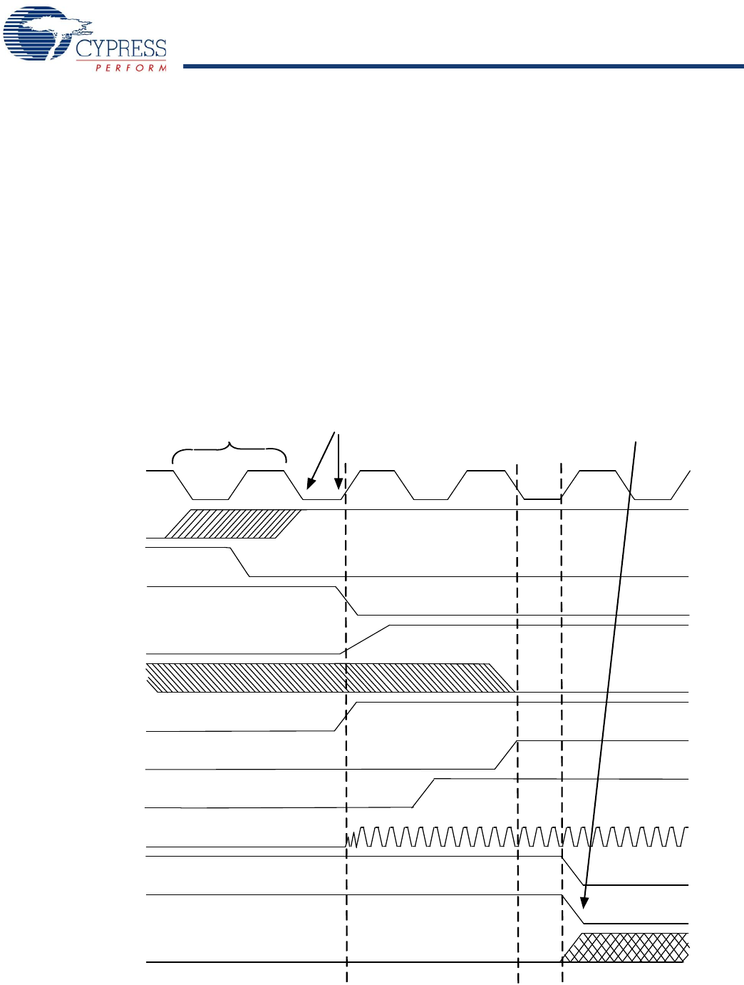
in Figure 14-2., the wakeup sequence is as follows:
1. The wakeup interrupt occurs and is synchronized by the neg-
ative edge of the 32 kHz clock.
2. At the following positive edge of the 32 kHz clock, the system
wide PD signal is negated. The Flash memory module,
internal oscillator, EFTB, and bandgap circuit are all powered
up to a normal operating state.
3. At the following positive edge of the 32 kHz clock, the current
values for the precision POR and LVD have settled and are
sampled.
4. At the following negative edge of the 32 kHz clock (after about
15 µs nominal), the BRQ signal is negated by the sleep logic
circuit. On the following CPUCLK, BRA is negated by the CPU
and instruction execution resumes. Note that in Figure 14-2.
fixed function blocks, such as Flash, internal oscillator, EFTB,
and bandgap, have about 15 µs start up. The wakeup times
(interrupt to CPU operational) range from 75 µs to 105 µs.
Figure 14-2. Wakeup Timing
INT
SLEEP
PD
BANDGAP
CLK32K
SAMPLE
SAMPLE LVD/
POR
CPUCLK/
24MHz
BRA
BRQ
ENABLE
CPU
(Not to Scale)
Sleep Timer or GPIO
interrupt occurs
Interrupt is double sampled by
32K clock and PD is negated to
system
CPU is restarted after
90ms (nominal)
[+] Feedback [+] Feedback


