CY7C68053
Document # 001-06120 Rev *F Page 12 of 39
4.1 CY7C68053 Pin Descriptions
Note
9. Unused inputs must not be left floating. Tie either HIGH or LOW as appropriate. Outputs should only be pulled up or down to ensure signals at power up and
in standby. Note also that no pins should be driven while the device is powered down
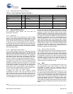
Table 4-1. FX2LP18 Pin Descriptions
[9]
56 VFBGA Name Type Default Description
2D AV
CC
Power N/A Analog VCC. Connect this pin to 3.3V power source. This signal provides
power to the analog section of the chip.
Appropriate bulk/bypass capacitance should be provided for this
supply rail.
1D AV
CC
Power N/A Analog VCC. Connect this pin to 3.3V power source. This signal provides
power to the analog section of the chip.
2F AGND Ground N/A Analog Ground. Connect this pin to ground with as short a path as
possible.
1F AGND Ground N/A Analog Ground. Connect to this pin ground with as short a path as
possible.
1E DMINUS I/O/Z Z USB D– Signal. Connect this pin to the USB D– signal.
2E DPLUS I/O/Z Z USB D+ Signal. Connect this pin to the USB D+ signal.
8B RESET# Input N/A Active LOW Reset. This pin resets the entire chip. See Section 3.9 ”Reset
and Wakeup” on page 5 for more details.
1C XTALIN Input N/A Crystal Input. Connect this signal to a 24 MHz parallel resonant, funda-
mental mode crystal and load capacitor to GND.
It is also correct to drive XTALIN with an external 24-MHz square wave
derived from another clock source.
2C XTALOUT Output N/A Crystal Output. Connect this signal to a 24 MHz parallel resonant, funda-
mental mode crystal and load capacitor to GND.
If an external clock is used to drive XTALIN, leave this pin open.
2B CLKOUT O/Z 12 MHz CLKOUT. 12-, 24- or 48-MHz clock, phase locked to the 24 MHz input
clock. The 8051 defaults to 12 MHz operation. The 8051 may tri-state this
output by setting CPUCS.1 = 1.
Port A
8G PA0 or
INT0#
I/O/Z I
(PA0)
Multiplexed pin whose function is selected by PORTACFG.0
PA0 is a bidirectional IO port pin.
INT0# is the active LOW 8051 INT0 interrupt input signal, which is either
edge triggered (IT0 = 1) or level triggered (IT0 = 0).
6G PA1 or
INT1#
I/O/Z I
(PA1)
Multiplexed pin whose function is selected by:
PORTACFG.1
PA1 is a bidirectional IO port pin.
INT1# is the active LOW 8051 INT1 interrupt input signal, which is either
edge triggered (IT1 = 1) or level triggered (IT1 = 0).
8F PA2 or
SLOE
I/O/Z I
(PA2)
Multiplexed pin whose function is selected by two bits:
IFCONFIG[1:0].
PA2 is a bidirectional IO port pin.
SLOE is an input-only output enable with programmable polarity
(FIFOPINPOLAR.4) for the slave FIFO’s connected to FD[7:0] or FD[15:0].
7F PA3 or
WU2
I/O/Z I
(PA3)
Multiplexed pin whose function is selected by:
WAKEUP.7 and OEA.3
PA3 is a bidirectional IO port pin.
WU2 is an alternate source for USB Wakeup, enabled by WU2EN bit
(WAKEUP.1) and polarity set by WU2POL (WAKEUP.4). If the 8051 is in
suspend and WU2EN = 1, a transition on this pin starts up the oscillator
and interrupts the 8051 to allow it to exit the suspend mode. Asserting this
pin inhibits the chip from suspending, if WU2EN = 1.
[+] Feedback


