CY7C68053
Document # 001-06120 Rev *F Page 9 of 39
3.14.1 Three Control OUT Signals
The 56-pin package brings out three of these signals,
CTL0–CTL2. The 8051 programs the GPIF unit to define the
CTL waveforms. CTLx waveform edges can be programmed
to make transitions as fast as once per clock cycle (20.8 ns
using a 48 MHz clock).
3.14.2 Two Ready IN Signals
The FX2LP18 package brings out all two Ready inputs
(RDY0–RDY1). The 8051 programs the GPIF unit to test the
RDY pins for GPIF branching.
3.14.3 Long Transfer Mode
In master mode, the 8051 appropriately sets GPIF transaction
count registers (GPIFTCB3, GPIFTCB2, GPIFTCB1, or
GPIFTCB0) for unattended transfers of up to 2
32
transactions.
The GPIF automatically throttles data flow to prevent under or
overflow until the full number of requested transactions
complete. The GPIF decrements the value in these registers
to represent the current status of the transaction.
3.15 ECC Generation
[6]
The MoBL-USB can calculate Error Correcting Codes (ECC’s)
on data that passes across its GPIF or Slave FIFO interfaces.
There are two ECC configurations: two ECC’s, each calculated
over 256 bytes (SmartMedia Standard) and one ECC calcu-
lated over 512 bytes.
The ECC can correct any 1-bit error or detect any 2-bit error.
3.15.1 ECC Implementation
The two ECC configurations are selected by the ECCM bit.
3.15.1.1 ECCM = 0
Two 3-byte ECC’s are each calculated over a 256-byte block
of data. This configuration conforms to the SmartMedia
Standard.
This configuration writes any value to ECCRESET, then
passes data across the GPIF or Slave FIFO interface. The
ECC for the first 256 bytes of data is calculated and stored in
ECC1. The ECC for the next 256 bytes is stored in ECC2. After
the second ECC is calculated, the values in the ECCx registers
do not change until ECCRESET is written again, even if more
data is subsequently passed across the interface.
3.15.1.2 ECCM = 1
One 3-byte ECC is calculated over a 512-byte block of data.
This configuration writes any value to ECCRESET then
passes data across the GPIF or Slave FIFO interface. The
ECC for the first 512 bytes of data is calculated and stored in
ECC1; ECC2 is unused. After the ECC is calculated, the value
in ECC1 does not change until ECCRESET is written again,
even if more data is subsequently passed across the interface.
3.16 USB Uploads and Downloads
The core has the ability to directly edit the data contents of the
internal 16-kByte RAM and of the internal 512-byte scratch
pad RAM via a vendor-specific command. This capability is
normally used when ‘soft’ downloading user code and is
available only to and from internal RAM, only when the 8051
is held in reset. The available RAM spaces are 16 kBytes from
0x0000–0x3FFF (code/data) and 512 bytes from
0xE000–0xE1FF (scratch pad data RAM).
[7]
3.17 Autopointer Access
FX2LP18 provides two identical autopointers. They are similar
to the internal 8051 data pointers, but with an additional
feature: they can optionally increment after every memory
access.The autopointers are available in external FX2LP18
registers, under control of a mode bit (AUTOPTRSET-UP.0).
Using the external FX2LP18 autopointer access (at 0xE67B –
0xE67C) allows the autopointer to access all RAM. Also, the
autopointers can point to any FX2LP18 register or endpoint
buffer space.
3.18 I
2
C Controller
FX2LP18 has one I
2
C port that is driven by two internal
controllers. One automatically operates at boot time to load the
VID/PID/DID, configuration byte, and firmware and a second
controller that the 8051, once running, uses to control external
I
2
C devices. The I
2
C port operates in master mode only.
3.18.1 I
2
C Port Pins
The I
2
C pins SCL and SDA must have external 2.2K ohm pull
up resistors even if no EEPROM is connected to the FX2LP18.
The value of the pull up resistors required may vary, depending
on the combination of V
CC_IO
and the supply used for the
EEPROM. The pull up resistors used must be such that when
the EEPROM pulls SDA low, the voltage level meets the V
IL
specification of the FX2LP18. For example, if the EEPROM
runs off a 3.3V supply and V
CC_IO
is 1.8V, the pull up resistors
recommended are 10K ohm. This requirement may also vary
depending on the devices being run on the I
2
C pins. Refer to
the I
2
C specifications for details.
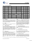
External EEPROM device address pins must be configured
properly. See Table 3-6 for configuring the device address
pins.
If no EEPROM is connected to the I
2
C port, EEPROM
emulation is required by an external processor.This is because
the FX2LP18 comes out of reset with the DISCON bit set, so
the device will not enumerate without an EEPROM (C2 load)
or EEPROM emulation.
Notes
6. To use the ECC logic, the GPIF or Slave FIFO interface must be configured for byte-wide operation.
7. After the data has been downloaded from the host, a ‘loader’ can execute from internal RAM in order to transfer downloaded data to external memory.
[+] Feedback


