CY7C68053
Document # 001-06120 Rev *F Page 2 of 39
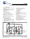
Cypress Semiconductor Corporation’s MoBL-USB FX2LP18
(CY7C68053) is a low-voltage (1.8 volt) version of the EZ-
USB
®
FX2LP (CY7C68013A), which is a highly integrated,
low-power USB 2.0 microcontroller. By integrating the USB 2.0
transceiver, serial interface engine (SIE), enhanced 8051
microcontroller, and a programmable peripheral interface in a
single chip, Cypress has created a very cost-effective solution
that provides superior time-to-market advantages with low
power to enable bus powered applications.
The ingenious architecture of MoBL-USB FX2LP18 results in
data transfer rates of over 53 Mbytes per second, the
maximum allowable USB 2.0 bandwidth, while still using a low-
cost 8051 microcontroller in a package as small as a 56
VFBGA (5 mm x 5 mm). Because it incorporates the USB 2.0
transceiver, the MoBL-USB FX2LP18 is more economical,
providing a smaller footprint solution than USB 2.0 SIE or
external transceiver implementations. With MoBL-USB
FX2LP18, the Cypress Smart SIE handles most of the USB 1.1
and 2.0 protocol in hardware, freeing the embedded microcon-
troller for application-specific functions and decreasing devel-
opment time to ensure USB compatibility.
The General Programmable Interface (GPIF) and
Master/Slave Endpoint FIFO (8- or 16-bit data bus) provide an
easy and glueless interface to popular interfaces such as
ATA,
UTOPIA, EPP, PCMCIA, and most DSP/processors.
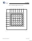
The 56VFBGA package is defined for the family.
The MoBL-USB FX2LP18 is also referred to as FX2LP18 in
this document.
2.0 Applications
There are a wide variety of applications for the MoBL-USB
FX2LP18. It is used in cell phone, smart phones, PDAs, and
MP3 players, to name a few.
The ‘Reference Designs’ section of the Cypress web site
provides additional tools for typical USB 2.0 applications. Each
reference design comes complete with firmware source and
object code, schematics, and documentation. For more infor-
mation, visit http://www.cypress.com.
3.0 Functional Overview
The functionality of this chip is described in the sections below.
3.1 USB Signaling Speed
FX2LP18 operates at two of the three rates defined in the USB
Specification Revision 2.0, dated April 27, 2000.
• Full-speed, with a signaling bit rate of 12 Mbps
• High-speed, with a signaling bit rate of 480 Mbps.
FX2LP18 does not support the low-speed signaling mode of
1.5 Mbps.
3.2 8051 Microprocessor
The 8051 microprocessor embedded in the FX2LP18 family
has 256 bytes of register RAM, an expanded interrupt system,
and three timer/counters.
3.2.1 8051 Clock Frequency
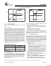
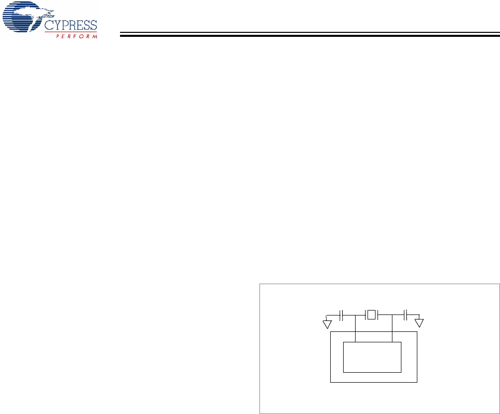
FX2LP18 has an on-chip oscillator circuit that uses an external
24 MHz (±100-ppm) crystal with the following characteristics:
• Parallel resonant
• Fundamental mode
• 500 µW drive level
• 12 pF (5% tolerance) load capacitors
An on-chip PLL multiplies the 24 MHz oscillator up to 480 MHz,
as required by the transceiver/PHY; internal counters divide it
down for use as the 8051 clock. The default 8051 clock
frequency is 12 MHz. The clock frequency of the 8051 can be
changed by the 8051 through the CPUCS register, dynami-
cally.
The CLKOUT pin, which can be tri-stated and inverted using
internal control bits, outputs the 50% duty cycle 8051 clock, at
the selected 8051 clock frequency — 48, 24, or 12 MHz.
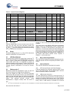
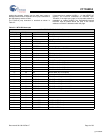
3.2.2 Special Function Registers
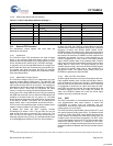
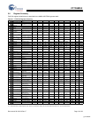
Certain 8051 Special Function Register (SFR) addresses are
populated to provide fast access to critical FX2LP18 functions.
These SFR additions are shown in Table 3-1. Bold type
indicates non-standard, enhanced 8051 registers. The two
SFR rows that end with ‘0’ and ‘8’ contain bit-addressable
registers. The four IO ports A – D use the SFR addresses used
in the standard 8051 for ports 0 – 3, which are not implemented
in FX2LP18. Because of the faster and more efficient SFR
addressing, the FX2LP18 IO ports are not addressable in
external RAM space (using the MOVX instruction).
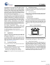
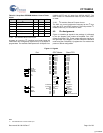
Figure 3-1. Crystal Configuration
12 pf
12 pf
24 MHz
20 × PLL
C1
C2
12 pF capacitor values assumes a trace capacitance
of 3 pF per side on a four-layer FR4 PCA
[+] Feedback


