


CYV15G0104TRB
Document #: 38-02100 Rev. *B Page 11 of 27
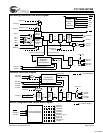
INSELA input. The Serial Line Receiver inputs are differential,
and can accommodate wire interconnect and filtering losses
or transmission line attenuation greater than 16 dB. For
normal operation, these inputs should receive a signal of at
least VI
DIFF
> 100 mV, or 200 mV peak-to-peak differential.
Each Line Receiver can be DC- or AC-coupled to +3.3V
powered fiber-optic interface modules (any ECL/PECL family,
not limited to 100K PECL) or AC-coupled to +5V powered
optical modules. The common-mode tolerance of these line
receivers accommodates a wide range of signal termination
voltages. Each receiver provides internal DC-restoration, to
the center of the receiver’s common mode range, for AC-
coupled signals.
Signal Detect/Link Fault
Each selected Line Receiver (i.e., that routed to the clock and
data recovery PLL) is simultaneously monitored for
• analog amplitude above amplitude level selected by
SDASELA
• transition density above the specified limit
• range controls report the received data stream inside
normal frequency range (±1500 ppm
[24]
)
• receive channel enabled
• Presence of reference clock
•ULCA
is not asserted.
All of these conditions must be valid for the Signal Detect block
to indicate a valid signal is present. This status is presented on
the LFIA
(Link Fault Indicator) output associated with each
receive channel, which changes synchronous to the receive
interface clock.
Analog Amplitude
While most signal monitors are based on fixed constants, the
analog amplitude level detection is adjustable to allow
operation with highly attenuated signals, or in high-noise
environments. The analog amplitude level detection is set by
the SDASELA latch via device configuration interface. The
SDASELA latch sets the trip point for the detection of a valid
signal at one of three levels, as listed in Table 2. This control
input affects the analog monitors for all receive channels. The
Analog Signal Detect monitors are active for the Line Receiver
as selected by the INSELA input.
Transition Density
The Transition Detection logic checks for the absence of
transitions spanning greater than six transmission characters
(60 bits). If no transitions are present in the data received, the
Detection logic for that channel asserts LFIA
.
Range Controls
The CDR circuit includes logic to monitor the frequency of the
PLL Voltage Controlled Oscillator (VCO) used to sample the
incoming data stream. This logic ensures that the VCO
operates at, or near the rate of the incoming data stream for
two primary cases:
• when the incoming data stream resumes after a time in
which it has been “missing.”
• when the incoming data stream is outside the acceptable
signaling rate range.
To perform this function, the frequency of the RXPLL VCO is
periodically compared to the frequency of the TRGCLKA±
input. If the VCO is running at a frequency beyond
±1500ppm
[24]
as defined by the TRGCLKA± frequency, it is
periodically forced to the correct frequency (as defined by
TRGCLKA±, SPDSELA, and TRGRATEA) and then released
in an attempt to lock to the input data stream.
The sampling and relock period of the Range Control is calcu-
lated as follows: RANGE_CONTROL_ SAMPLING_PERIOD
= (RECOVERED BYTE CLOCK PERIOD) * (4096).
During the time that the Range Control forces the RXPLL VCO
to track TRGCLKA±, the LFIA
output is asserted LOW. After a
valid serial data stream is applied, it may take up to one
RANGE CONTROL SAMPLING PERIOD before the PLL
locks to the input data stream, after which LFIA
should be
HIGH.
The operating serial signaling-rate and allowable range of
TRGCLKA± frequencies are listed in Table 3.
Receive Channel Enabled
The receive channel can be enabled or disabled through the
RXPLLPDA input latch as controlled by the device configu-
ration interface. When RXPLLPDA = 0, the CDR PLL and
analog circuitry of the channel are disabled. Any disabled
channel indicates a constant link fault condition on the LFIA
output. When RXPLLPDA = 1, the CDR PLL and receive
channel are enabled to receive a serial stream.
Note. When the disabled receive channel is reenabled, the
status of the LFIA
output and data on the parallel outputs for
the associated channel may be indeterminate for up to 2 ms.
Clock/Data Recovery
The extraction of a bit-rate clock and recovery of bits from the
received serial stream is performed by a separate CDR block
within the receive channel. The clock extraction function is
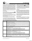
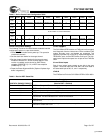
Table 2. Analog Amplitude Detect Valid Signal Levels
[7]
SDASELA
Typical Signal with Peak Amplitudes
Above
00 Analog Signal Detector is disabled
01 140 mV p-p differential
10 280 mV p-p differential
11 420 mV p-p differential
Note:
7. The peak amplitudes listed in this table are for typical waveforms that have generally 3–4 transitions for every ten bits. In a worse case environment the signals
may have a sine-wave appearance (highest transition density with repeating 0101...). Signal peak amplitudes levels within this environment type could increase
the values in the table above by approximately 100 mV.
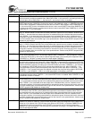
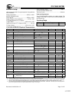
Table 3. Operating Speed Settings
SPDSELA TRGRATEA
TRGCLKA±
Frequency
(MHz)
Signaling
Rate (Mbps)
LOW
1 reserved 195–400
0 19.5–40
MID (Open) 1 20–40 400–800
0 40–80
HIGH 1 40–75 800–1500
0 80–150
[+] Feedback