


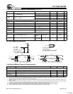

CYV15G0104TRB
Document #: 38-02100 Rev. *B Page 14 of 27
RXPLLPDA Receive Channel Enable. The initialization value of the RXPLLPDA latch = 0. RXPLLPDA selects if the
receive channel is enabled or powered-down. When RXPLLPDA = 0, the receive PLL and analog circuitry are
powered-down. When RXPLLPDA = 1, the receive PLL and analog circuitry are enabled.
RXBISTA[1:0] Receive Bist Disable / SMPTE Receive Enable. The initialization value of the RXBISTA[1:0] latch = 11. For
SMPTE data reception, RXBISTA[1:0] should not remain in this initialization state (11). RXBISTA[1:0] selects
if receive BIST is disabled or enabled and sets the device for SMPTE data reception. When RXBISTA[1:0] =
01, the receiver BIST function is disabled and the device is set to receive SMPTE data. When RXBISTA[1:0]
= 10, the receive BIST function is enabled and the device is set to receive BIST data. RXBISTA[1:0] = 00 and
RXBISTA[1:0] = 11 are invalid states.
ROE2A Reclocker Secondary Differential Serial Data Output Driver Enable. The initialization value of the ROE2A
latch = 0. ROE2A selects if the ROUTA2± secondary differential output drivers are enabled or disabled. When
ROE2A = 1, the associated serial data output driver is enabled allowing the reclocked data to be transmitted.
When ROE2A = 0, the associated serial data output driver is disabled. When a driver is disabled via the
configuration interface, it is internally powered down to reduce device power. If both serial drivers for a channel
are in this disabled state, the reclocker logic is also powered down. A device reset (RESET sampled LOW)
disables all output drivers.
ROE1A Reclocker Primary Differential Serial Data Output Driver Enable. The initialization value of the ROE1A
latch = 0. ROE1A selects if the ROUTA1± primary differential output drivers are enabled or disabled. When
ROE1A = 1, the associated serial data output driver is enabled allowing the reclocked data to be transmitted.
When ROE1A = 0, the associated serial data output driver is disabled. When a driver is disabled via the
configuration interface, it is internally powered down to reduce device power. If both serial drivers for a channel
are in this disabled state, the reclocker logic is also powered down. A device reset (RESET sampled LOW)
disables all output drivers.
TXCKSELB Transmit Clock Select. The initialization value of the TXCKSELB latch = 1. TXCKSELB selects the clock
source used to write data into the Transmit Input Register. When TXCKSELB = 1, the input register TXDB[9:0]
is clocked by REFCLKB↑. In this mode, the phase alignment buffer in the transmit path is bypassed. When
TXCKSELB = 0, TXCLKB↑ is used to clock in the input register TXDB[9:0].
TXRATEB Transmit PLL Clock Rate Select. The initialization value of the TXRATEB latch = 0. TXRATEB is used to
select the clock multiplier for the Transmit PLL. When TXRATEB = 0, the transmit PLL multiples the REFCLKB±
input by 10 to generate the serial bit-rate clock. When TXRATEB = 0, the TXCLKOB output clocks are full-rate
clocks and follow the frequency and duty cycle of the REFCLKB± input. When TXRATEB = 1, the Transmit
PLL multiplies the REFCLKB± input by 20 to generate the serial bit-rate clock. When TXRATEB = 1, the
TXCLKOB output clocks are twice the frequency rate of the REFCLKB± input. When TXCKSELB = 1 and
TXRATEB = 1, the Transmit Data Inputs are captured using both the rising and falling edges of REFCLKB.
TXRATEB = 1 and SPDSELB = LOW, is an invalid state and this combination is reserved.
TXBISTB Transmit Bist Disable. The initialization value of the TXBISTB latch = 1. TXBISTB selects if the transmit BIST
is disabled or enabled. When TXBISTB = 1, the transmit BIST function is disabled. When TXBISTB = 0, the
transmit BIST function is enabled.
TOE2B
Secondary Differential Serial Data Output Driver Enable. The initialization value of the TOE2B latch = 0.
TOE2B selects if the TOUTB2± secondary differential output drivers are enabled or disabled. When TOE2B
= 1, the associated serial data output driver is enabled allowing data to be transmitted from the transmit shifter.
When TOE2B = 0, the associated serial data output driver is disabled. When a driver is disabled via the
configuration interface, it is internally powered down to reduce device power. If both serial drivers for a channel
are in this disabled state, the associated internal logic for that channel is also powered down. A device reset
(RESET sampled LOW) disables all output drivers.
TOE1B Primary Differential Serial Data Output Driver Enable. The initialization value of the TOE1B latch = 0.
TOE1B selects if the TOUTB1± primary differential output drivers are enabled or disabled. When TOE1B = 1,
the associated serial data output driver is enabled allowing data to be transmitted from the transmit shifter.
When TOE1B = 0, the associated serial data output driver is disabled. When a driver is disabled via the
configuration interface, it is internally powered down to reduce device power. If both serial drivers for a channel
are in this disabled state, the associated internal logic for that channel is also powered down. A device reset
(RESET sampled LOW) disables all output drivers.
PABRSTB Transmit Clock Phase Alignment Buffer Reset. The initialization value of the PABRSTB latch = 1. The
PABRSTB is used to re-center the Transmit Phase Align Buffer. When the configuration latch PABRSTB is
written as a 0, the phase of the TXCLKB input clock relative to REFCLKB+/- is initialized. PABRSTB is an
asynchronous input, but is sampled by each TXCLKB↑ to synchronize it to the internal clock domain.
PABRSTB is a self clearing latch. This eliminates the requirement of writing a 1 to complete the initialization
of the Phase Alignment Buffer.
Table 4. Device Configuration and Control Latch Descriptions (continued)
Name Signal Description
[+] Feedback