


CYV15G0104TRB
Document #: 38-02100 Rev. *B Page 18 of 27
V
OLC
Output LOW Voltage
(V
CC
Referenced)
100Ω differential load V
CC
– 1.4 V
CC
– 0.7 V
150Ω differential load V
CC
– 1.4 V
CC
– 0.7 V
V
ODIF
Output Differential Voltage
|(OUT+) − (OUT−)|
100Ω differential load 450 900 mV
150Ω differential load 560 1000 mV
Differential Serial Line Receiver Inputs: INA1±, INA2±
V
DIFFs
[9]
Input Differential Voltage |(IN+) − (IN−)| 100 1200 mV
V
IHE
Highest Input HIGH Voltage V
CC
V
V
ILE
Lowest Input LOW Voltage V
CC
– 2.0 V
I
IHE
Input HIGH Current V
IN
= V
IHE
Max. 1350 µA
I
ILE
Input LOW Current V
IN
= V
ILE
Min. –700 µA
VI
COM
[11]
Common Mode input range ((V
CC
– 2.0V)+0.5)min,
(V
CC
– 0.5V) max.
+1.25 +3.1 V
Power Supply Typ. Max.
I
CC
[12, 13]
Max Power Supply Current REFCLKB
= MAX
Commercial 585 690 mA
I
CC
[12, 13]
Typical Power Supply Current REFCLKB
= 125 MHz
Commercial 560 660 mA
CYV15G0104TRB DC Electrical Characteristics (continued)
Parameter Description Test Conditions Min. Max. Unit
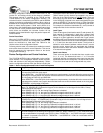
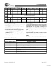
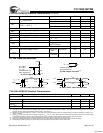
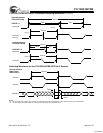
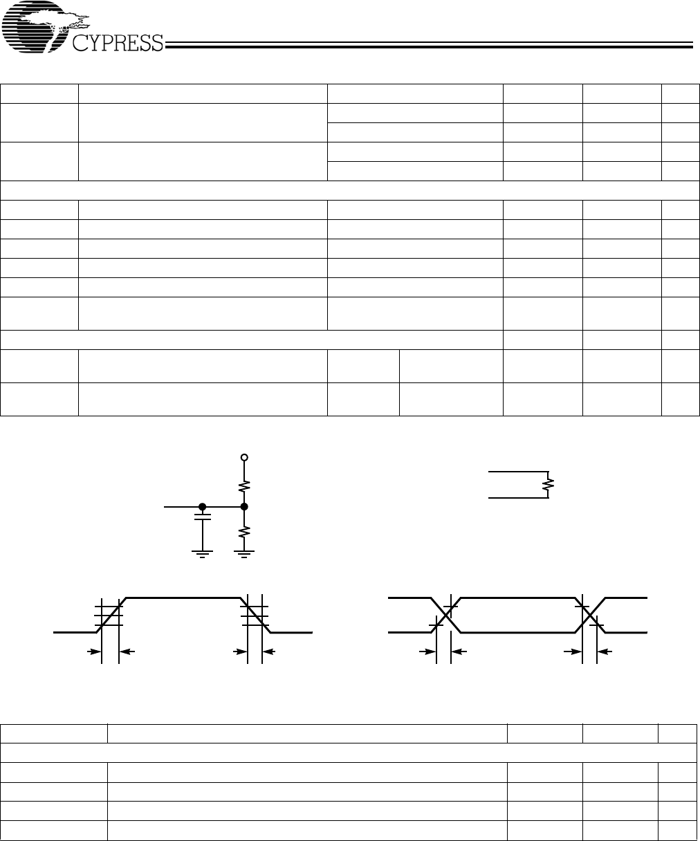
AC Test Loads and Waveforms
2.0V
0.8V
GND
2.0V
0.8V
80%
20%
80%
20%
R
L
(Includes fixture and
probe capacitance)
3.0V
V
th
=1.4V
≤ 270 ps
≤ 270 ps
[15]
V
th
=1.4V
3.3V
R1
R2
R1 = 590Ω
R2 = 435Ω
(Includes fixture and
probe capacitance)
C
L
≤ 7 pF
(a) LVTTL Output Test Load
R
L
= 100Ω
(b) CML Output Test Load
C
L
(c) LVTTL Input Test Waveform
(d) CML/LVPECL Input Test Waveform
≤ 1ns
≤ 1 ns
V
IHE
V
ILE
V
IHE
V
ILE
[14]
[14]
CYV15G0104TRB AC Electrical Characteristics
Parameter Description Min. Max Unit
CYV15G0104TRB Transmitter LVTTL Switching Characteristics Over the Operating Range
f
TS
TXCLKB Clock Cycle Frequency 19.5 150 MHz
t
TXCLK
TXCLKB Period=1/f
TS
6.66 51.28 ns
t
TXCLKH
[16]
TXCLKB HIGH Time 2.2 ns
t
TXCLKL
[16]
TXCLKB LOW Time 2.2 ns
Notes:
11. The common mode range defines the allowable range of INPUT+ and INPUT− when INPUT+ = INPUT−. This marks the zero-crossing between the true and
complement inputs as the signal switches between a logic-1 and a logic-0.
12. Maximum I
CC
is measured with V
CC
= MAX,T
A
= 25°C, with all channels and Serial Line Drivers enabled, sending a continuous alternating 01 pattern, and
outputs unloaded.
13. Typical I
CC
is measured under similar conditions except with V
CC
= 3.3V, T
A
= 25°C,with all channels enabled and one Serial Line Driver per channel sending
a continuous alternating 01 pattern. The redundant outputs on each channel are powered down and the parallel outputs are unloaded.
14. Cypress uses constant current (ATE) load configurations and forcing functions. This figure is for reference only.
15. The LVTTL switching threshold is 1.4V. All timing references are made relative to where the signal edges cross the threshold voltage.
16. Tested initially and after any design or process changes that may affect these parameters, but not 100% tested.
[+] Feedback