


CYV15G0104TRB
Document #: 38-02100 Rev. *B Page 12 of 27
performed by an integrated PLL that tracks the frequency of
the transitions in the incoming bit stream and aligns the phase
of the internal bit-rate clock to the transitions in the selected
serial data stream.
Each CDR accepts a character-rate (bit-rate
÷ 10) or half-
character-rate (bit-rate
÷ 20) training clock from the
TRGCLKA± input. This TRGCLKA± input is used to
• ensure that the VCO (within the CDR) is operating at the
correct frequency (rather than a harmonic of the bit-rate)
• reduce PLL acquisition time
• limit unlocked frequency excursions of the CDR VCO when
there is no input data present at the selected Serial Line
Receiver.
Regardless of the type of signal present, the CDR attempts to
recover a data stream from it. If the signaling rate of the
recovered data stream is outside the limits set by the range
control monitors, the CDR tracks TRGCLKA± instead of the
data stream. Once the CDR output (RXCLKA±) frequency
returns back close to the TRGCLKA± frequency, the CDR
input is switched back to the input data stream. If no data is
present at the selected line receiver, this switching behavior
may result in brief RXCLKA± frequency excursions from
TRGCLKA±. However, the validity of the input data stream is
indicated by the LFIA
output. The frequency of TRGCLKA± is
required to be within ±1500ppm
[24]
of the frequency of the
clock that drives the REFCLKB± input of the remote trans-
mitter to ensure a lock to the incoming data stream. This large
ppm tolerance allows the CDR PLL to reliably receive a 1.485
or 1.485/1.001 Gbps SMPTE HD-SDI data stream with a
constant TRGCLK frequency.
For systems using multiple or redundant connections, the
LFIA
output can be used to select an alternate data stream.
When an LFIA
indication is detected, external logic can toggle
selection of the INA1± and INA2± input through the INSELA
input. When a port switch takes place, it is necessary for the
receive PLL for that channel to reacquire the new serial
stream.
Reclocker
The receive channel performs a reclocker function on the
incoming serial data. To do this, the Clock and Data Recovery
PLL first recovers the clock from the data. The data is retimed
by the recovered clock and then passed to an output register.
Also, the recovered character clock from the receive PLL is
passed to the reclocker output PLL which generates the bit
clock that is used to clock the retimed data into the output
register. This data stream is then transmitted through the
differential serial outputs.
Reclocker Serial Output Drivers
The serial output interface drivers use differential Current
Mode Logic (CML) drivers to provide source-matched drivers
for 50Ω transmission lines. These drivers accept data from the
reclocker output register in the reclocker channel. These
drivers have signal swings equivalent to that of standard PECL
drivers, and are capable of driving AC-coupled optical
modules or transmission lines.
Reclocker Output Channels Enabled
Each driver can be enabled or disabled separately via the
device configuration interface.
When a driver is disabled via the configuration interface, it is
internally powered down to reduce device power. If both
reclocker serial drivers are in this disabled state, the internal
reclocker logic is also powered down. The deserialization logic
and parallel outputs will remain enabled. A device reset
(RESET
sampled LOW) disables all output drivers.
Note. When the disabled reclocker function (i.e., both outputs
disabled) is re-enabled, the data on the reclocker serial
outputs may not meet all timing specifications for up to 250 µs.
Output Bus
The receive channel presents a 10-bit data signal (and a BIST
status signal when RXBISTA[1:0] = 10).
Receive BIST Operation
The receiver channel contains an internal pattern checker that
can be used to validate both device and link operation. These
pattern checkers are enabled by the RXBISTA[1:0] latch via
the device configuration interface. When enabled, a register in
the receive channel becomes a signature pattern generator
and checker by logically converting to a Linear Feedback Shift
Register (LFSR). This LFSR generates a 511-character
sequence. This provides a predictable yet pseudo-random
sequence that can be matched to an identical LFSR in the
attached Transmitter(s). When synchronized with the received
data stream, the Receiver checks each character from the
deserializer with each character generated by the LFSR and
indicates compare errors and BIST status at the RXDA[1:0]
and BISTSTA bits of the Output Register.
The BIST status bus {BISTSTA, RXDA[0], RXDA[1]} indicates
010b or 100b for one character period per BIST loop to
indicate loop completion. This status can be used to check test
pattern progress.
The specific status reported by the BIST state machine is listed
in Table 6. These same codes are reported on the receive
status outputs.
If the number of invalid characters received ever exceeds the
number of valid characters by 16, the receive BIST state
machine aborts the compare operations and resets the LFSR
to look for the start of the BIST sequence again.
A device reset (RESET
sampled LOW) presets the BIST
Enable Latches to disable BIST on all channels.
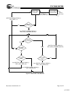
BIST Status State Machine
When a receive path is enabled to look for and compare the
received data stream with the BIST pattern, the {BISTSTA,
RXDA[1:0]} bits identify the present state of the BIST compare
operation.
The BIST state machine has multiple states, as shown in
Figure 2 and Table 6. When the receive PLL detects an out-of-
lock condition, the BIST state is forced to the Start-of-BIST
state, regardless of the present state of the BIST state
machine. If the number of detected errors ever exceeds the
number of valid matches by greater than 16, the state machine
is forced to the WAIT_FOR_BIST state where it monitors the
receive path for the first character of the next BIST sequence.
Power Control
The CYV15G0104TRB supports user control of the powered
up or down state of each transmit and receive channel. The
receive channels are controlled by the RXPLLPDA latch via
[+] Feedback