


EM78612
Universal Serial Bus Microcontroller
Product Specification (V1.0) 03.22.2006 •
••
• 13
(This specification is subject to change without further notice)
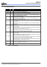
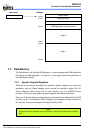
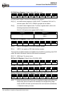
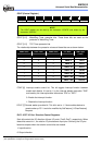
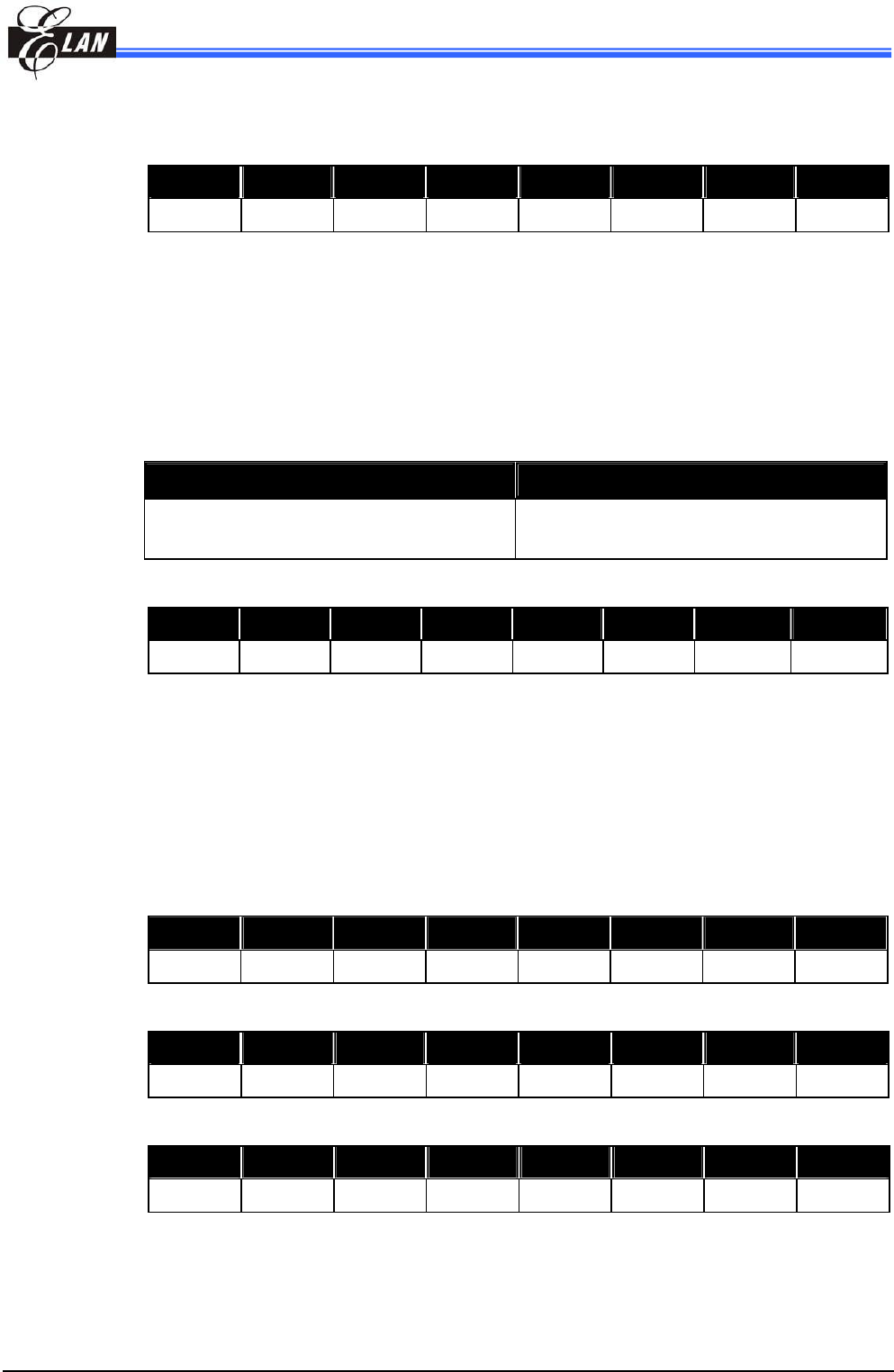
R4 (RAM Select Register) Default Value: (0B_0xxx_xxxx)
7 6 5 4 3 2 1 0
- BK0 Ad5 Ad4 Ad3 Ad2 Ad1 Ad0
R4 (RAM select register) contains the address of the registers.
R4 [0~5] are used to select registers in 0x00h~0x3Fh. The address 0x00~0x1F is
common space. After 0x1Fh, SRAM is grouped into two banks.
R4 [6] are used to select register banks. To select a registers bank, refer to the
following examples and the table below:
R4=01111100 points to the register 0x3C in Bank 1.
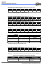
R4[6]Bk0 RAM Bank #
0
1
Bank 0
Bank 1
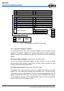
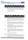
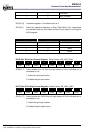
R5 (Data Line I/O Register) Default Value: (0B_0000_0000)
7 6 5 4 3 2 1 0
- - - - - - D- or DATA D+ or CLK
R5 [0] USB D+ line register or PS/2 clock interface register.
R5 [1] USB D- line register or PS/2 data interface register.
These two bits are BOTH writable and readable when the MCU is operating under PS/2
mode. But under USB Mode, these two bits cannot be accessed.
R5 [2~7] NON Used .The value is zero.
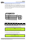
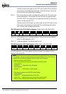
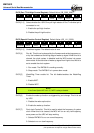
R6 (Port 6 I/O Register) Default Value: (0B_0000_0000)
7 6 5 4 3 2 1 0
P67 P66 P65 P64 P63 P62 P61 P60
R7 (Port 7 I/O Register) Default Value: (0B_0000_0000)
7 6 5 4 3 2 1 0
- - - - P73 P72 P71 P70
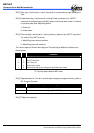
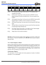
R8 (Port 6 Wake-up Pin Selection Register) Default Value: (0B_1111_1111)
7 6 5 4 3 2 1 0
/Wu67 /wu66 /Wu65 /Wu64 /Wu63 /Wu62 /Wu61 /Wu60
R8 [0 ~ 7] Select which of the Port 6 pins are to be defined to wake-up the MCU from
sleep mode. When the state of the selected pins changes during sleep
mode, the MCU will wake-up and execute the next instruction automatically.
1: Disable the wake-up function