


EM78612
Universal Serial Bus Microcontroller
32 •
••
• Product Specification(V1.0) 03.22.2006
(This specification is subject to change without further notice)
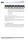
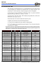
B. Instruction Set
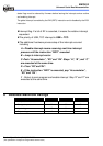
Each instruction in the instruction set is a 11-bit word divided into an OP code and one
or more operands. All instructions are executed within one single instruction cycle
(consisting of 2 oscillator periods), unless the program counter is changed by-
(a) Executing the instruction "MOV R2,A", "ADD R2,A", "TBL", or any other instructions
that write to R2 (e.g. "SUB R2,A", "BS R2,6", "CLR R2", ⋅⋅⋅⋅).
(b) execute CALL, RET, RETI, RETL, JMP, Conditional skip (JBS, JBC, JZ, JZA, DJZ,
DJZA) which were tested to be true.
Under these cases, the execution takes two instruction cycles.
In addition, the instruction set has the following features:
(1). Every bit of any register can be set, cleared, or tested directly.
(2). The I/O register can be regarded as general register. That is, the same instruction
can operate on I/O register.
The symbol "R" represents a register designator that specifies which one of the registers (including operational
registers and general purpose registers) is to be utilized by the instruction. Bits 6 and 7 in R4 determine the selected
register bank. "b" represents a bit field designator that selects the value for the bit located in the register "R" and
affects operation. "k" represents an 8 or 10-bit constant or literal value.
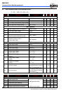
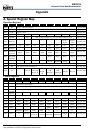
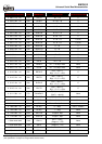
INSTRUCTION BINARY HEX MNEMONIC OPERATION STATUS AFFECTED
0 0000 0000 0000 0000 NOP No Operation None
0 0000 0000 0001 0001 DAA Decimal Adjust A C
0 0000 0000 0010 0002 CONTW A → CONT None
0 0000 0000 0011 0003 SLEP 0 → WDT, Stop oscillator T,P
0 0000 0000 0100 0004 WDTC 0 → WDT T,P
0 0000 0000 rrrr 000r IOW R A → IOCR None <Note1>
0 0000 0001 0000 0010 ENI Enable Interrupt None
0 0000 0001 0001 0011 DISI Disable Interrupt None
0 0000 0001 0010 0012 RET [Top of Stack] → PC None
0 0000 0001 0011 0013 RETI
[Top of Stack] → PC,
Enable Interrupt
None
0 0000 0001 0100 0014 CONTR CONT → A None
0 0000 0001 rrrr 001r IOR R IOCR → A None <Note1>
0 0000 0010 0000 0020 TBL
R2+A → R2,
Bits 8~9 of R2 unchanged
Z,C,DC
0 0000 01rr rrrr 00rr MOV R,A A → R None
0 0000 1000 0000 0080 CLRA 0 → A Z
0 0000 11rr rrrr 00rr CLR R 0 → R Z
0 0001 00rr rrrr 01rr SUB A,R R-A → A Z,C,DC
0 0001 01rr rrrr 01rr SUB R,A R-A → R Z,C,DC
0 0001 10rr rrrr 01rr DECA R R-1 → A Z