


EM78612
Universal Serial Bus Microcontroller
Product Specification (V1.0) 03.22.2006 •
••
• 15
(This specification is subject to change without further notice)
Therefore, before writing data into the FIFO, the firmware will first check this
bit to prevent overwriting the existing data. These two bits can only be set
by the firmware and cleared by the hardware.
RC [7] EP0_W flag. After the UDC completes writing data to the FIFO, this bit will
be set automatically. The firmware will clear it as soon as it gets the data
from EP0’s FIFO. Only when this bit is cleared that the UDC will be able to
write a new data into the FIFO.
Therefore, before the firmware can write a data into the FIFO, this bit must
first be set by the firmware to prevent UDC from writing data at the same
time. This bit is both readable and writable.
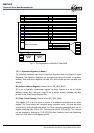
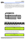
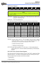
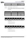
RD (USB Application FIFO Address Register) Default Value: (0B_0000_0000)
7 6 5 4 3 2 1 0
0 0 0 UAD4 UAD3 UAD2 UAD1 UAD0
RD [0~4] USB Application FIFO address registers. These five bits are the address
pointer of USB Application FIFO.
RD [5~7] Undefined registers. The default value is zero.
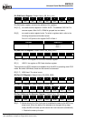
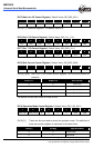
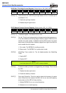
RE (USB Application FIFO Data Register) Default Value: (0B_0000_0000)
7 6 5 4 3 2 1 0
UD7 UD6 UD5 UD4 UD3 UD2 UD1 UD0
RE (USB Application FIFO data register) contains the data in the register of which
address is pointed by RD.
NOTE
For example, if we want to read the fourth byte of the EndPoint Zero, we will use the
address of EP0 (0x00) and Data Byte Pointer of EP0 (0x10) to access it.
// Read the 4rd byte of the EP0 FIFO
// First, assign the data byte pointer of EP0 register (0X10) with 0X03.
MOVA, @0X10
MOVRD, a // Move data in A to RD register
MOVA, @0X03
MOVRE , A // Move data in A to RE register
// Then read the content from EP0 FIFO (0x00) 4rd byte
MOVA, @0X00
MOVRD, A // Assign address point to EP0 FIFO
MOVA, RE // Read the fourth byte data (byte3) of the EP0 FIFO
MOV A, 0X0E// Read the fifth byte data (byte4) of the EP0 FIFO