


©2002 Fairchild Semiconductor Corporation Application Note 7511 Rev. A1
Latch-Up: Hints, Kinks and Caveats
The IGT is a rugged device, requiring no snubber network
when operating within its published safe-operating-area
(SOA) ratings. Within the SOA, the gate emitter voltage
controls the collector current. In fact, the IGT can conduct
three to four times the published maximum current if it’s in the
ON state and the junction temperature is +150
o
C maximum.
However, if the current exceeds the rated maximum, the IGT
could lose gate control and latch up during turn-off attempts.
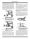
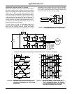
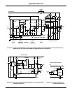
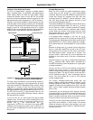
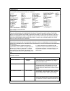
The culprit is the parasitic SCR formed by the pnpn structure
shown in Figure 16. In the equivalent circuit, Q
1
is a power
MOSFET with a normal parasitic transistor (Q
2
) whose base-
emitter junction is shunted by the low-value resistance R
1
.
FIGURE 16. THE IGT’S PARASITIC SCR IS RESPONSIBLE FOR
THE DEVICE’S LATCH-UP CHARACTERISTICS.
For large current overloads, the current flowing through R
1
can provoke SCR triggering. In the simplest terms, R
1
repre-
sents the equivalent of a distributed resistor network, whose
magnitude is a function of Q
2
’s V
CE
. During normal IGT
operation, a positive gate voltage (greater than the thresh-
old) applied between Q
1
’s gate and source turns the FET on.
The FET then turns on Q
3
(a pnp transistor with very low
gain), causing a small portion of the total collector current to
flow through the R
1
network.
To turn the IGT off, you must reduce the gate-to-emitter
voltage to zero. This turns Q
1
off, thus initiating the turn-off
sequence within the device. Total fall time includes current-
fall-time one (t
F1
) and current-fall-time two (t
F2
)
components. The turn-off is a function of the gate-emitter
resistance, Q
3
’s storage time and the value of V
GE
prior to
turn-off. Device characteristics fix both the delay time and
the fall time.
Forward-Bias Latch-Up
Within the IGT’s current and junction-temperature ratings,
current does not flow through Q
2
under forward-biased
conditions. When the current far exceeds its rated value, the
current flow through R
1
increases and Q
3
’s V
CE
also
increases because of MOSFET channel saturation. Once
Q
3
’s I
C
R
1
drop exceeds Q
2
’s V
BE(ON)
, Q
2
turns on and
more current flow bypasses the FET.
The positive feedback thus established causes the device to
latch in the forward-biased mode. The value of I
C
at which
the IGT latches on while in forward conduction is typically
three to four times the device’s maximum rated collector
current. When the collector current drops below the value
that provokes Q
2
turn-on, normal operation resumes if chip
temperature is still within ratings.
If the gate-to-emitter resistance is too low, the Q
2
-Q
3
parasitic SCR can cause the IGT to latch up during turn-off.
During this period, R
GE
determines the drain-source dV/dt of
power MOSFET Q
1
. A low R
1
causes a rapid rise in voltage -
this increases Q
2
’s V
CE
, increasing both R
1
’s value and Q
2
’s
gain.
Because of storage time, Q
3
’s collector current continues to
flow at a level that’s higher than normal for the FET bias.
During rapid turn-off, a portion of this current could flow in
Q
2
’s base-emitter junction, causing Q
2
to conduct. This
process results in device latch-up; current distribution will
probably be less uniform than in the case of forward-bias
latch-up.
Because the gains of Q
2
and Q
3
increase with temperature
and V
CE
, latching current - high at +25
o
C - decreases as a
function of increasing junction temperature for a given gate-
to-emitter resistance.
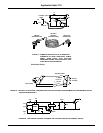
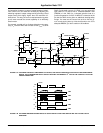
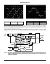
How do you test an IGT’s turn-off latching characteristic?
Consider the circuit in Figure 17. Q
1
’s base-current pulse
width is set approximately 2µsec greater than the IGT’s gate-
voltage pulse width. This way, the device under test (DUT)
can be switched through Q
1
when reverse-bias latch-up
occurs. This circuit allows you to test an IGT’s latching
current nondestructively.
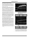
The results? Clamped-inductive-load testing with and
without snubbers reveals that snubbering increases current
handling dramatically: With RGE = 1kΩ, a 0.02µF snubber
capacitor increases current capability from 6A to 10A; with
RGE = 5kΩ, a 0.09µF snubber practically doubles capacity
(25A vs 13A).
Conclusions? You can double the IGT’s latching current by
increasing RGE from 1kΩ to 5kΩ, and double it again with a
polarized snubber using CS < 0.1µF. The IGT is therefore
useful in situations where the device must conduct currents
of five to six times normal levels for short periods.
Finally, you can also use the latching behavior to your advan-
tage under fault conditions. In other words, if the device
latches up during turn-off under normal operation, you could
arrange it so that a suitable snubber is switched electroni-
cally across the IGT.
EMITTER METAL POLYSILICON GATE
P
METAL COLLECTOR
MINORITY
CARRIER
INJECTION
MAIN CURRENT PATH
N EPITAXIAL LAYER
P+ SUBSTRATE
N+N+
P
COLLECTOR
Q
3
R
1
EMITTER
GATE
Q
2
Q
1
Application Note 7511