


©2002 Fairchild Semiconductor Corporation Application Note 7511 Rev. A1
Piezoelectric Couplers Provide 4-kV Isolation
Using a high-frequency oscillator for pulse-train drive Figure
6B yields unlimited on-time capability. However, the scheme
requires an oscillator that can be turned on and off by the
control logic. A diode or zener clamp across the trans-
former’s primary will limit leakage-inductance flyback effects.
To optimize transformer efficiency, make the pulses’ voltage
x time products equal for both the On and the Off pulses. In
situations where the line voltage generates the drive power,
a simple relaxation oscillator using a programmable unijunc-
tion transistor can derive its power directly from the line to
provide a pulse train to the IGT gate.
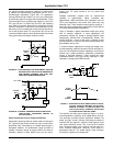
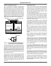
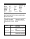
The circuit shown in Figure 7 accommodates applications
involving lower frequencies (a few hundred Hertz and
below). The high oscillator frequency (greater than 20kHz)
helps keep the pulse transformer reasonably small. The volt-
age-doubler circuitry improves the turn-on time and also pro-
vides long on-time capability. Although this design uses only
a 5V supply on the primary side of a standard trigger trans-
former, it provides 15V gate-to-emitter voltage.
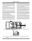
FIGURE 7. THIS DRIVING METHOD FOR LOW-FREQUENCY
SWITCHING PROVIDES 15V TO THE IGT’S GATE
OSCILLATOR
1:2
1N914
0.001µF
4.7k
0.001
µF
IGT
1N914
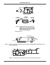
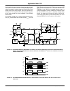
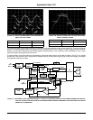
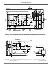
FIGURE 9A. THE POWER INVERTER’S DRIVE CIRCUIT USES SIX IGTS TO DRIVE A 2-HP MOTOR.
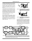
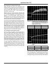
FIGURE 9B. THE TIMING DIAGRAM SHOWS THAT EACH IGT
CONDUCTS FOR 165
o×
OF EVERY 360
o
CYCLE;
THE DELAY IS NECESSARY TO AVOID CROSS
CONDUCTION.
FIGURE 9C. THE THREE WINDINGS’ VOLTAGES AND CUR-
RENTS ARE SHOWN. NOTE THAT ALTHOUGH
COSTLY SNUBBER NETWORKS ARE ELIMINAT-
ED, FREEWHEELING DIODES ARE NEEDED; THE
IGTS HAVE NO INTRINSIC OUTPUT DIODE.
INDUCTION
MOTOR
D
7
325V
10A
NOTES:
Q
1
- Q
6
= D94FR4
D
1
- D
7
= 1N3913
D
8
- D
13
= 1N914
R = 4.7k,
1
/
2
W
C
1
= 100µF, 400V
L
1
= 40µH
220V
L
1
D
1
D
2
Q
2
Q
1
R
R
C
1
D
3
D
5
Q
3
Q
5
RR
RR
Q
4
Q
6
D
4
D
6
t
t
t
t
t
t0
0
0
0
0
0
φA
φB
φC
I
LA
I
LB
I
LC
Q
1
ON
Q
2
ON
Q
3
ON
180
o
15
o
DELAY
Q
4
ON
Q
5
ON
Q
6
ON
V
AB
0t
V
BC
V
CA
I
LA
I
LB
I
LC
0
0
0
0
0
t
t
t
t
t
Application Note 7511