


Function Description
Readout Module876A-1
4
4-3
High Voltage Power Supply Normal Operation (non-ECS Test)
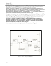
The multivibrator circuit of Q7 and Q8 also supplies the input to the high voltage generator. Two of the
transistors of U1 act as buffers between the multivibrator and the high voltage circuit. Q4 and Q3 serve an
output driving stage for the primary of high voltage transformer T1. The input to T1 is a square wave,
approximately 12.5 V peak to peak. T1 has a step-up ratio of approximately 20: 1. C22, CR15, CR14, and
C20 form a voltage doubler that gives a DC output of approximately 525 volts. The resistor capacitor
circuit R42, R43, and R44, and C17, C18, and C19 serve for further filtering, and ultimately a 506 volt
output is delivered at J1.
R37, R40 and R41 form a voltage divider across the 515 V input to the resistor capacitor filter. The
voltage at the junction of R37 and R40 is the input to OP AMP U2 pins 6 through series resistor R39. Pins
5 and 6 of U2 are the inputs to a difference amplifier, which acts to produce additional regulation of the
high voltage.
U2 (pins 1, 2, 3) is used as a logic circuit in the SAFE/FAIL circuit of the monitor, refer to FAIL/SAFE
Comparison Circuit on Power Supply Board for additional information. In addition to the 6.2 V
reference signal, a voltage will be present at terminal P that comes from terminal 8 of the ECS board
during the ECS test, and a muting signal will also be present at terminal M. This circuit is a part of a
complex checking circuit during the ECS test, and is described in more detail in the "FAIL/SAFE"
paragraph.
Operation of High Voltage Supply During ECS Test
A low voltage ramp (approximately 0 to 6.2 V) from the ECS board enters the power supply board on
terminal 12, and proceeds through a series of auxiliary circuits to give a ramp of the same waveshape on
the center-tap of the primary of high voltage transformer T1, which point is also the source of power to the
driving circuit Q3 and Q4. As a result of this variation of the voltage at the center-tap, the amplitude of the
current in the primary varies accordingly, and ultimately the voltage output at J1 varies from 0 to 506
volts, linearly with time. This high voltage ramp generates the current in the detector circuit during the
ECS test period.
FAIL/SAFE Comparison Circuit on Power Supply Board
The comparison circuit on the power supply board, consisting of U2, pins 1, 2, and 3 has two functions:
The first function, a monitoring of the high voltage, is in operation at all times except during the ECS test.
If this voltage falls below 80% of its rated value, (roughly, from 500 to 400 volts), the FAIL/SAFE circuit
will go out, and the FAIL relay will de-energize. During this period, a steady 6.2 volts, which is input on
terminal 13, serves as a comparison voltage. The voltage on pin 2 is proportional to the high voltage
through a high ratio voltage divider.
The second function, a monitoring of the result of the ECS test, is in operation during this test. During this
period, the high voltage falls well below 400 volts (actually, practically to zero) so the monitoring of the
high voltage as in the above paragraph is inapplicable. Instead, the following are the input and output
conditions.
On pin 2 there is impressed a positive 15-volt signal that lasts for the duration of the ECS test (6.0
seconds). The voltage on terminal M is 15 volts during the ECS test and zero at all other times. The wave
shape that creates this condition on terminal M is called the muting signal wave shape. It will override
whatever voltage would otherwise be present through the high ratio voltage divider from J1.
On pin 3 of the comparison circuit there is impressed a DC voltage that is either 6.2 volts (safe condition)
or 15 volts (fail condition). This voltage arrives on terminal P of the power supply board from a latch circuit
on the ECS board, which circuit will be described in connection with that board. A safe condition causes
the output on terminal N (from pin 1 of U2) to be -10 volts; a fail condition causes it to be +15 volts.
Terminal N is connected to the SAFE/FAIL circuit on the relay driver board, which controls the action of
the fail relay and the SAFE-RESET green lamp on the panel. A fail condition causes the green lamp to go
out and de-energizes the fail relay, although the muting signal delays these actions until the end of the six
(6) second ECS test period. For the safe condition the green light is on, and the fail relay is energized.