Processor Thermal/Mechanical Information
12 Thermal and Mechanical Design Guidelines
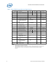
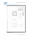
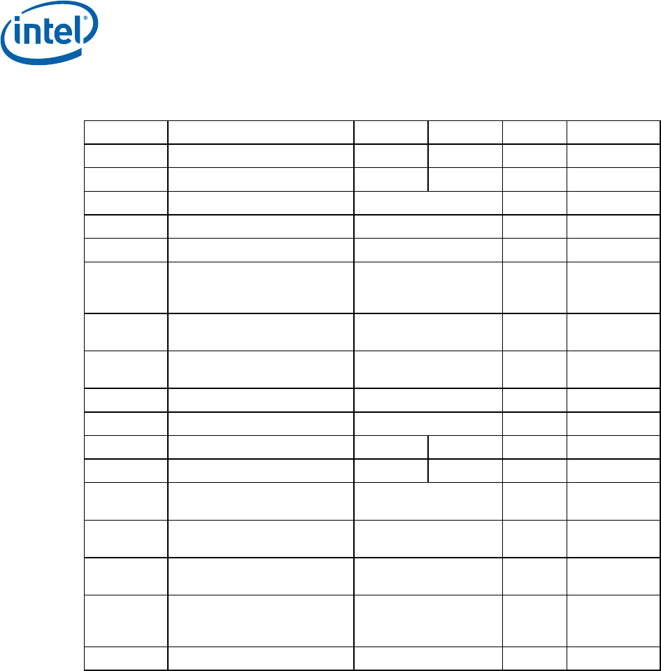
Table 1. Micro-FCBGA Package Mechanical Specifications
Symbol Parameter Min Max Unit Figure
B1 Package substrate width 34.95 35.05 mm Figure 2
B2 Package substrate length 34.95 35.05 mm Figure 2
C1 Die width 11.1 mm Figure 2
C2 Die length 8.2 mm Figure 2
F2 Die height (with underfill)
0.89 mm Figure 2
F3 Package overall height
(package substrate to
die)
2.022 Max mm
Figure 2
G1 Width (first ball center to
last ball center)
31.75 Basic mm Figure 2
G2 Length (first ball center
to last ball center)
31.75 Basic mm Figure 2
J1 Ball pitch (horizontal) 1.27 Basic mm Figure 2
J2 Ball pitch (vertical) 1.27 Basic mm Figure 2
M Solder Resist Opening 0.61 0.69 mm Figure 2
N Ball height 0.6 0.8 mm Figure 2
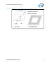
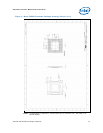
-- Corner Keep-out zone at
corner (4X)
7 × 7 mm Figure 3
-- Keep-out from edge of
package (4X)
5 mm Figure 3
-- Package edge to first ball
center
1.625 mm Figure 3
P
die
Allowable pressure on
the die for thermal
solution
689 kPa
W Package weight 6 g
NOTE:
1. All dimensions are subject to change.
2. Overall height as delivered. Values were based on design specifications and tolerances.
Final height after surface mount depends on OEM motherboard design and SMT
process.


