


Intel
®
21143 PCI/CardBus 10/100Mb/s Ethernet LAN Controller
14 Design Guide
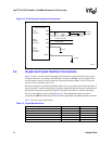
3.2.3 100-Ready External Module Design
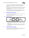
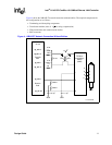
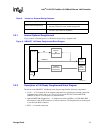
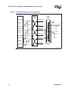
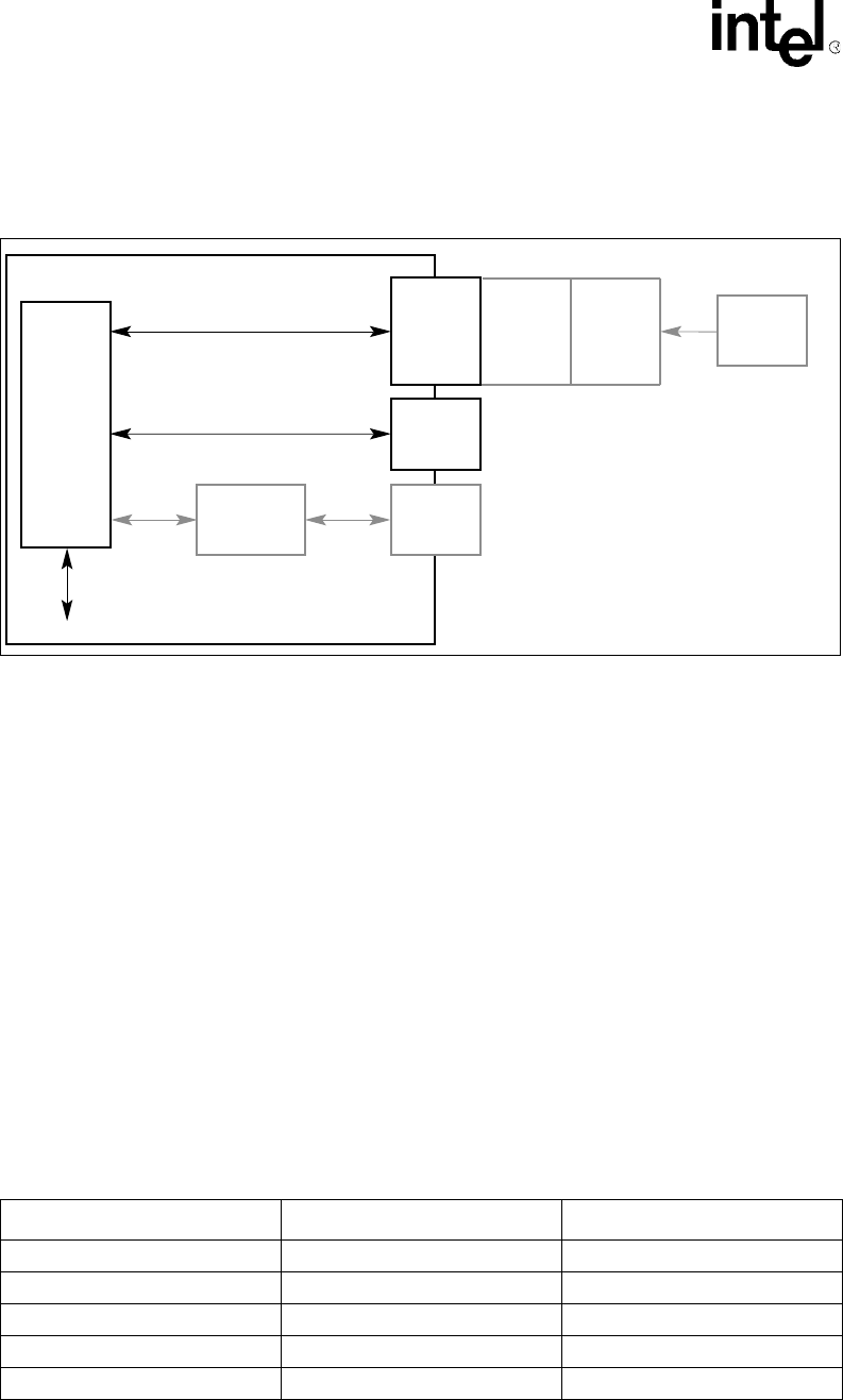
Figure 7 shows a block diagram of a 100-Ready design using an external module.
3.2.4 Description of 100-Ready External Module Block Diagram
The blocks in the100-Ready external module block diagram represent the following components:
• 21143 — A 21143 with all of the external components for operating the network connection
(reference parts, XTAL, and so on). The 21143 can use the PCI bus, and the MII/SYM,
10BASE-T, and AUI coaxial ports for communication.
• Optional external MII/SYM daughtercard — A daughtercard with a 100 Mb/s or 10/100 Mb/s
PHY that interfaces with an MII connector or custom connector. The daughtercard uses the
magnetics to connect to the RJ45 connector.
• MII connector — An MII or custom connector that connects with the MII/SYM port of the 21143.
• RJ45 — A network connection.
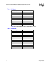
3.2.5 MII/SYM Pin Listing
Table 7 describes the MII/SYM pin multiplexing enabling the full flexibility for both network
connections options using the same internal connector for the MII-based or the SYM-based PHY
device (for detailed implementation notes, refer to the specific PHY device section in this document).
Figure 7. 10BASE-T 100-Ready External Module Block Diagram
LJ-05188.AI4
PCI
Bus
Optional
AUI Coaxial
Transceivers
MII or
Custom
Connector
RJ45
Connector
AUI
Coaxial
Connector
MII/SYM
10BASE-T
RJ45
Connector
10/100
PHY Layer
MII or
Custom
Connector
21143
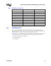
Table 7. MII/SYM Pinout (Sheet 1 of 2)
Pin Number MII Interface Function SYM Interface Function
117 mii_crs sd
118 mii_clsn sym_rxd<4>
119 mi_txd<3> sym_txd<3>
120 mi_txd<2> sym_txd<2>
121 mi_txd<1> sym_txd<1>