Intel
®
21143 PCI/CardBus 10/100Mb/s Ethernet LAN Controller
Design Guide 21
5.0 Signal Routing and Placement
The Ethernet circuitry should be kept free of interference from unrelated signal traces. Routing for
other signals must be kept away from the space surrounding the grouped Ethernet components. Place
the Ethernet circuitry at the perimeter of the board, as close as possible to the network connector.
The onchip crystal oscillator requires an external crystal and discrete components. For stable and
noise-free operation, place the crystal and discrete components as close as possible to the 21143,
keeping the etch length as short as possible. Do not route any noisy signals in this area.
The PCI pin ordering is fully compatible with the PCI specification recommendation and can be
easily routed within the specified etch limits of the PCI signals. This includes shared signal lengths
of up to 3.8 cm (1.5 in) and the clock signal length of 6.41 cm (2.5 in).
Keep all signal paths short and route them as directly as possible.
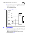
Systems using 10BASE-T nodes can be connected by cables up to 100 m (328 ft.). As a result, signals
that reach the board can be noisy and low in amplitude. To minimize corrupting this data, route these
signals, by most direct path, from the network connector and through the magnetics coupler to the 21143.
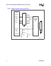
The length of this path should not exceed 8 cm (3 in) for the active AUI signals. The MII/SYM
interface operates at 25 MHz (or 2.5 MHz). All routing of the MII/SYM signals to the MII/SYM device
should be as short as possible and should not have significant differences of lengths and characteristics
within signal groups. Examples of signal groups include mii_rxd<4:0> and mii_txd<4:0>.
Note: The routing of these signals should be done with caution. The preferred routing of these signals is
in the external routing layers of the board. The MII/SYM device should be located between the
21143 and the magnetics port.
5.1 Ground and Power Planes
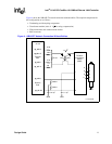
Up to four types of power signals require handling when implementing a design with the 21143:
• Gnd is adapter ground.
• Vcc (+5 V from PCI) drives the external components (boot ROM and Ethernet address ROM).
• Vdd (+3.3 V) drives the 21143.
• Vee (-9 V output) power from the DC-to-DC converter if the coaxial network connection is
implemented. For information specific to the -9 V power supply, refer to the transceiver used
to drive the coaxial network connection.
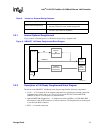
Intel recommends that at least two power planes be kept on the PCB: Vcc and Gnd. The Vdd
power plane (+3.3 V) can be implemented either by a cut in the Vcc power plane, or by a power
island under the 21143 on one of the signal routing layers.
Intel recommends that decoupling capacitors should be connected to all power supplies. These
capacitors should be placed as close as possible to the power pins of the chips. The recommended
values are as follows: 0.1 µF, 0.01 µF, 10 µF (tantalum), and 47 µF (tantalum).
For better noise-testing immunity, separate all power planes between the network connectors and
the transformer from the logic and analog power planes of the adapter for the 10BASE-T,
10BASE2, 100BASE-T4, and 100BASE-TX connections.


