


Design Guide 3
Contents
Contents
1.0 Functional Overview ........................................................................................................................5
1.1 21143 Overview....................................................................................................................5
1.2 Network Interface..................................................................................................................5
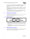
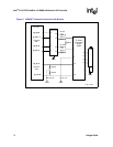
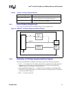
1.3 MII-Based PHY Block Diagram.............................................................................................6
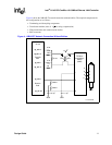
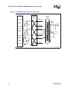
1.4 SYM-Based PHY Block Diagram..........................................................................................6
2.0 21143 Ports .....................................................................................................................................7
3.0 Network Connection ........................................................................................................................9
3.1 10BASE-T Twisted-Pair Network Port ..................................................................................9
3.2 100-Ready Designs ............................................................................................................12
3.2.1 Internal Optional Daughtercard..............................................................................13
3.2.2 Description of 100-Ready Daughtercard Block Diagram .......................................13
3.2.3 100-Ready External Module Design ......................................................................14
3.2.4 Description of 100-Ready External Module Block Diagram...................................14
3.2.5 MII/SYM Pin Listing ...............................................................................................14
3.3 AUI Network Port ................................................................................................................15
3.4 Media-Specific Components...............................................................................................18
4.0 21143 Requirements .....................................................................................................................19
4.1 Unused JTAG Port Requirements ......................................................................................19
4.2 Current Reference and Capacitor Input Requirements ......................................................19
4.3 Crystal and Crystal Oscillator Connections ........................................................................20
5.0 Signal Routing and Placement ......................................................................................................21
5.1 Ground and Power Planes..................................................................................................21
5.1.1 3.3 V Power Supply ...............................................................................................22
5.2 LED Status Signals.............................................................................................................22
6.0 Design Considerations ..................................................................................................................23
6.1 Designing the Ethernet Corner on Motherboards ...............................................................23
6.2 Suggestions for FCC Compliance ......................................................................................23
6.2.1 Suggestions for Quiet Ground and Power Planes .................................................23
6.2.2 Suggestions for Routing ........................................................................................24
Figures
1 MII-Based PHY Design.................................................................................................................6
2 SYM-Based PHY Design..............................................................................................................7
3 10BASE-T Network Connection with Buffers..............................................................................10
4 10BASE-T Network Connection Without Buffers........................................................................11
5 Minimum Components Required for 10BASE-T ........................................................................12
6 10BASE-T 100-Ready Daughtercard Block Diagram.................................................................13
7 10BASE-T 100-Ready External Module Block Diagram.............................................................14
8 AUI 10BASE5 Network and Pin Connections.............................................................................16