Advanced/ZP Technical Product Summary • Page 9
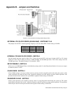
the CMOS RAM values can be cleared to the system defaults by using a configuration switch on the baseboard. Appendix
B lists switch and jumper configurations.
An external coin-cell style battery provides power to the RTC and CMOS memory. The battery has an estimated lifetime
of seven years and is socketed for easy replacement. Refer to Appendix A for battery replacement details.
IRDA (INFRARED) SUPPORT
Serial port 2 can be configured to support an IrDA module via a 5 pin header connector. Once configured for IrDA, the
user can transfer files to/from portable devices such as laptops, PDA’s and printers using application software such as
LapLink. The IrDA specification provides for data transfers at up to 115kbps from a distance of 1 meter.
A 5-pin header is provided to allow connection to a Hewlett Packard HSDSL-1000 compatible Infra-red
transmitter/receiver.
SYSTEM BIOS
The Advanced/ZP baseboard uses an American Megatrends Incorporated (AMI) Pentium Processor ROM BIOS, which is
stored in Flash EEPROM and easily upgraded using a floppy disk-based program. In addition to the AMIBIOS, the Flash
EEPROM also contains the Setup utility, Power-On Self Tests (POST), update recovery code, and the PCI auto-
configuration utility. This baseboard supports system BIOS shadowing, allowing the BIOS to execute from 32-bit on-
board write-protected DRAM.
The BIOS displays a sign-on message during POST identifying the type of BIOS and a five-digit revision code. As an
example the BIOS for the Advanced/ZE will be 1.00.02.BS0. As BIOS updates occur the revision number will increase to
1.00.03.BS0, and so on.
Information on BIOS functions can be found in the IBM PS/2 and Personal Computer BIOS Technical Reference
published by IBM, and the ISA and EISA Hi-Flex AMIBIOS Technical Reference published by AMI. Both manuals are
available at most technical bookstores.
FLASH IMPLEMENTATION
The Intel 28F001BXT 1 Mb FLASH component is organized as 128K x 8 (128 KB). The Flash device is divided into five
areas, as described in Table 1.
System Address
FLASH Memory Area
F0000H
FFFFFH
64 KB Main BIOS
EE000H EFFFFH 8 KB Boot Block (Not FLASH erasable)
ED000H EDFFFH 4 KB Plug and Play ESCD Storage Area
EC000H ECFFFH 4 KB OEM LOGO Area
E0000H EBFFFH 48 KB System BIOS Reserved
Table 2. Flash Memory Organization
The FLASH device resides in system memory in two 64 KB segments starting at E0000H, and can be mapped two
different ways, depending on the mode of operation. In Normal Mode, address line A16 is inverted, setting the E000H
and F000H segments so that the BIOS is organized as shown in the system address column above. Recovery mode
removes the inversion on address line A16, swapping the E000H and F000H segments so that the 8 KB boot block resides
at FE000H where the CPU expects the bootstrap loader to exist. This mode is only necessary in the unlikely event that a
BIOS upgrade procedure is interrupted, causing the BIOS area to be left in an unusable state. For information on
recovering the BIOS in the event of a catastrophic failure, refer to the appendix.
BIOS UPGRADES
FLASH memory makes distributing BIOS upgrades easy. A new version of the BIOS can be installed from a diskette.
BIOS upgrades will be available as downloadable files on the Intel bulletin board.
The disk-based Flash upgrade utility, FMUP.EXE, has three options for BIOS upgrades:


