


98 536EX Chipset Developer’s Manual
Intel Confidential
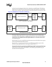
Parallel Host Interface 16C450/16C550A UART
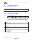
9.2.6 FIFO Control Register (FCR)
This write-only register is used to enable the receiver and transmitter FIFOs, clear the FIFOs, set
the RCVR FIFO trigger level, and select the DMA signaling type.
Bit 4
EPS (Even Parity Select)—When even parity select (LCR4) and parity enable (LCR3) are set to ‘1’, an even
number of logic 1’s are transmitted or checked. When even parity select (LCR4) is a ‘0’ and parity enable
(LCR3) is a ‘1’, an odd number of logic 1’s are transmitted or checked.
Bit 3
PEN (Parity Enable)—When this bit is set to ‘1’, a parity bit is generated (transmitted data) or checked
(receive data) between the last data character word bit and stop bit of the serial data.
NOTE: The parity bit is used to produce an even or odd number of 1’s when the data word bits and the parity
bits are summed.
Bit 2
Number of Stop Bits (STB)—This bit specifies the number of stop bits transmitted and received in each serial
character. When STB is set to ‘0’, one stop bit is generated for each transmitted data character. When STB is
set to ‘1’ and the word length (WLS1 and WLS0) is equal to 6, 7, or 8 bits, then two stop bits are generated for
each transmitted data character. When STB is set to ‘1’ and the word length (WLS1 and WLS0) is equal to 5
bits, then one and a half stop bits are generated for each transmitted data character. The receiver only checks
for the first stop bit, regardless of the number of stops bits transmitted.
Bits 1:0
Word Length Select Bits (WLS1 and WLS0)—These two bits specify the data character word length of the
transmitted and received data. The supported word lengths are provided below.
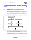
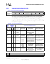
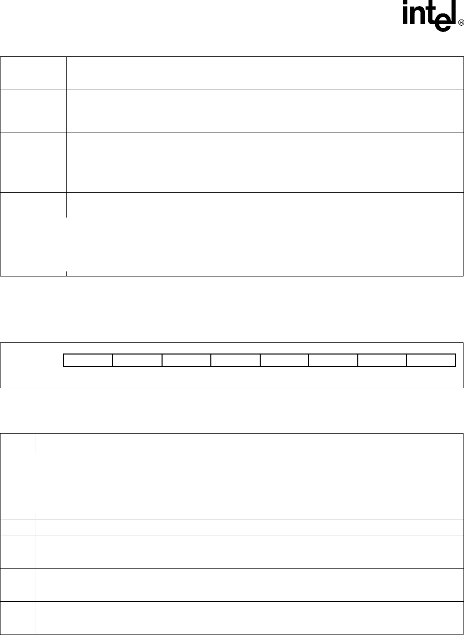
Figure 19. FIFO Control Register (FCR)
Bit 1 Bit 0 Word Length
00 5 bits
01 6 bits
10 7 bits
11 8 bits
RCVR Trig. RCVR Trig. Reserved Reserved DMA XFIFOR RFIFOR FIFOE
(write-only)
Register 2
Bits 7:6
MSB and LSB (RCVR Trigger Bits)—FCR bits 7 and 6 are used to set the trigger level for the RCVR FIFO interrupt.
Bits 5:3 Reserved—Bits 5, 4, and 3 are reserved for future enhancements.
Bit 2
XFIFOR (XMIT FIFO Reset)—When set to ‘1’, this bit clears all the bytes in the XMIT FIFO and resets the internal
counter logic to ‘0’. The internal shift register is not cleared by the XFIFOR bit. This bit is automatically cleared by the
modem.
Bit 1
RFIFOR (RCVR FIFO Reset)—When set to ‘1’, this bit clears all the bytes in the RCVR FIFO and resets the internal
counter logic to ‘0’. The internal shift register is not cleared by the RFIFOR bit. This bit is automatically cleared by the
modem.
Bit 0
FIFOE (FIFO Enable)—This bit when set to ‘1’, enables both the XMIT and RCVR FIFOs. This bit must be a ‘1’
whenever writing to any other FIFO bit. If FIFO is not set to ‘1’, then the DTE can not program any of the FIFO
functions.
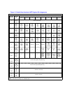
Bit 7 Bit 6
RCVR FIFO
Trigger Level (Bytes)
00 01
01 04
10 08
11 14