Chapter 1 Description of the GPIB-BUF
© National Instruments, Corp. 1-5 GPIB-BUF User Manual
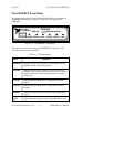
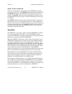
The port labeled GPIB IN is intended to be connected to a GPIB system that
includes one or more GPIB devices which send data to the GPIB target
device. All data received via the GPIB IN port is transferred into the
Random Access Memory (RAM) buffer of the GPIB-BUF using the on-
board Direct Memory Access (DMA) controller. The port labeled GPIB
OUT should be connected to the GPIB target device. This port has GPIB
controller capabilities and addresses the GPIB target device when required.
All data input to the internal GPIB-BUF RAM buffer is output via the GPIB
OUT port. Under normal operating conditions, you should only connect
one device (your GPIB target device) to the GPIB OUT port.
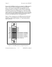
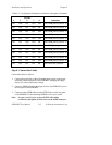
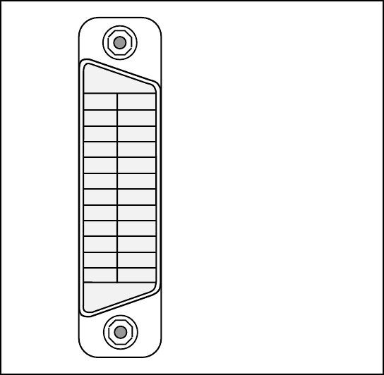
Figure 1-4 shows a diagram of one of the GPIB connectors and the signal
designations. Only one GPIB connector is shown since both connectors
have the same signal and pin descriptions. A * suffix indicates that the
signal is active low.
DIO1*
DIO2*
DIO3*
DIO4*
EOI*
DAV*
NRFD*
NDAC*
IFC*
SRQ*
ATN*
SHIELD
DIO5*
DIO6*
DIO7*
DIO8*
REN*
GND (Twisted Pair with DAV*)
GND (Twisted Pair with NRFD*)
GND (Twisted Pair with NDAC*)
GND (Twisted Pair with IFC*)
GND (Twisted Pair with SRQ*)
GND (Twisted Pair with ATN*)
SIGNAL GROUND
1
2
3
4
5
6
7
8
9
10
11
12
13
14
15
16
17
18
19
20
21
22
23
24
Figure 1-4. The GPIB Connector and Signal Designations


