


Chapter 5 Register Map and Description
©
National Instruments Corporation 5-3 PCI-DIO-96 User Manual
Register Descriptions
The register descriptions for the devices used on the PCI-DIO-96 are
given on the pages that follow. The register description bits labeled with
an X indicate don’t care bits. Always write a 0 to these bits.
Register Description Format
The remainder of this section discusses each of the PCI-DIO-96
registers in the order shown in Table 5-1. Each register group is
introduced, followed by a detailed bit description of each register.
Individual register descriptions give the address (in hexadecimal), type,
data size, and bit map of the register, followed by a description of each
bit.
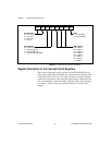
The register bit map shows a diagram of the register with the MSB
(bit 7) shown on the left, and the LSB (bit 0) shown on the right. A
rectangle with the bit name inside represents each bit.
The bit map for the Interrupt Clear Register states not applicable, no
bits used. The data is ignored when you write to this register; therefore,
any bit pattern will suffice.
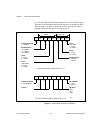
Register Description for the 82C55A
Figure 5-1 shows the two control word formats used to completely
program the 82C55A. The control word flag (bit 7) determines which
control word format is being programmed. When the control word flag
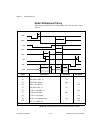
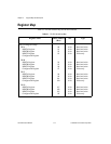
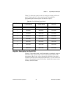
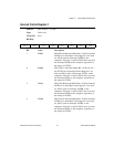
82C53 Register Group
PORTA Register
PORTB Register
PORTC Register
Configuration Register
10
11
12
13
8-bit
8-bit
8-bit
8-bit
Read-and-write
Read-and-write
Read-and-write
Write-only
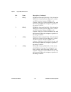
Interrupt Control Register Group
Register 1
Register 2
Interrupt Clear Register
14
15
16
8-bit
8-bit
8-bit
Write-only
Write-only
Write-only
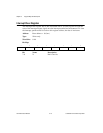
Table 5-1. PCI-DIO-96 Address Map (Continued)
Register Name Offset Address
(Hex)
Size Type