


Chapter 6 Programming
PCI-DIO-96 User Manual 6-16
©
National Instruments Corporation
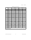
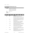
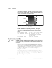
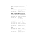
At the digital I/O connector, port C has the pin assignments shown in
Figure 6-6 when in mode 1 output. Notice that the status of ACKA* and
ACKB* are not included when port C is read.
Figure 6-6. Port C Pin Assignments on I/O Connector when Port C Configured for
Mode 1 Output
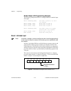
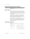
Mode 1 Strobed Output Programming Example
The following example shows how to configure PPI A for mode 1
output.
Write (8255Cnfg, 0xA0) Set mode 1-port A is an output
Loop until OBFA (PC7) is set, indicating that the
data last written to port A
has been read
Write (PortA, Data) Write data to port A
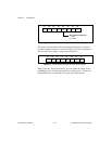
Mode 2–Bidirectional Bus
Note: For mode 2 examples, you must configure the don’t care bits appropriately
in the control word if you want to use the other ports in combination with
the example.
Mode 2 has an 8-bit bus that can transfer both input and output data
without changing the configuration. The data transfers are synchronized
with handshaking lines in port C. This mode uses only port A; however,
port B can be used in either mode 0 or mode 1 while port A is
configured for mode 2.
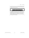
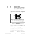
The control word written to the Configuration Register to configure
port A as a bidirectional data bus in mode 2 is shown in Figure 6-7. If
port B is configured for mode 0, you can use PC2, PC1, and PC0 of
port C as extra input or output lines.
PC7 OBFA*
PC6 ACKA*
PC5 I/O
PC4 I/O
PC3 INTRA
PC2 ACKB*
PC1 OBFB*
PC0 INTRB
Group A
Group B