


Chapter 2 Function Generator Operation
NI 5401 User Manual 2-2 www.natinst.com
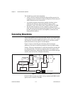
The NI 5401 has several main components:
• A PXI or PCI bus interface that handles Plug and Play protocols for
assigning resources to the device and providing drivers for the data and
address bus that are local to the device
• A waveform sequencer that performs multiple functions such as
arbitrating the data buses and controlling the triggers, filters,
attenuators, clocks, PLL, RTSI switch, instruction FIFO, and DDS
• The data from the memory is fed to a digital-to-analog converter
(DAC) through a half-band interpolating digital filter. The output from
the DAC goes through the filter to the amplifiers, attenuators, and,
finally, the I/O connector.
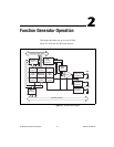
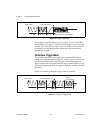
Generating Waveforms
The NI 5401 generates waveforms using DDS, which is used for generating
standard waveforms that are repetitive in nature, such as sine, TTL, square,
and triangular waveforms. DDS mode limits you to one buffer, and the
buffer size must be exactly equal to 16,384 samples.
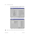
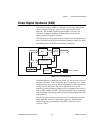
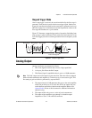
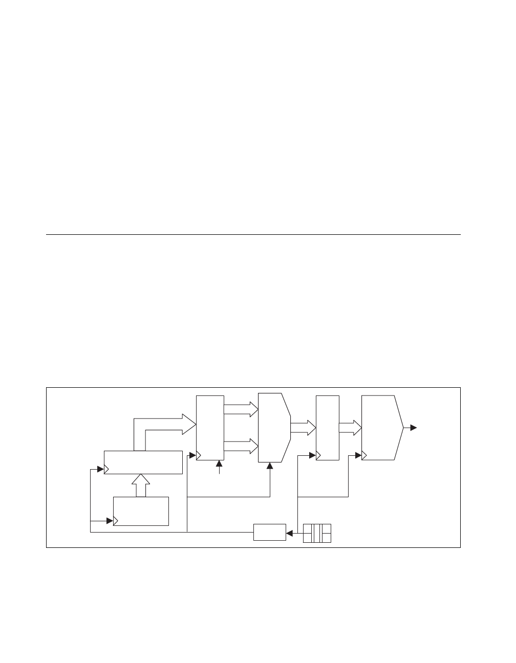
Figure 2-2 shows a block diagram of the data path for waveform
generation. The data for waveform generation comes from DDS lookup
memory. This data is interpolated by a half-band digital filter and then fed
to a high-speed DAC. The data has a pipeline delay of 26 update clocks
through this digital filter. Although the digital filter can be disabled through
software, there will still be a 26 update clock delay.
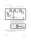
Figure 2-2.
Waveform Data Path Block Diagram
On the NI 5401, the high-speed DAC is always updated at 80 MHz, but the
update clock for memory is 40 MHz.
DDS Lookup
Memory
DDS
Digital Filter
Filter
MUX
A
B
12
DAC Register
80 MHz Oscillator
DAC12
12 Bits
Digital Filter
Enable
Div/2