Chapter 2 Function Generator Operation
©
National Instruments Corporation 2-15 NI 5401 User Manual
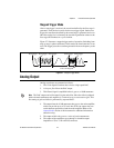
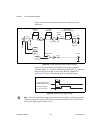
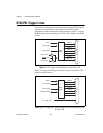
The NI 5401 can receive a hardware trigger from another board as a RTSI
trigger signal on any of the RTSI/PXI trigger lines.
You can also route signals as follows:
• Route the Start Trigger signal generated on the NI 5401 to other boards
through any of the RTSI/PXI bus trigger lines.
• Route the SYNC output generated on the NI 5401 to other boards
through any of the RTSI/PXI bus trigger lines.You can use this signal
to give other boards an accurate and fine frequency resolution clock.
♦ NI 5401 for PCI
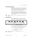
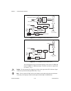
For frequency locking to other boards as a master, the NI 5401 sends an
onboard 20 MHz signal to the RTSI Osc line as a board clock signal. For
locking to other devices as a slave, the NI 5401 receives the RTSI Osc line
as a RTSI clock signal.
♦ NI 5401 for PXI
For frequency locking to other boards, the NI 5401 for PXI receives the
PXI backplane 10 MHz Osc as a reference clock signal. All the NI 5401s
for PXI use this common signal as the reference clock for frequency
locking.
Note Refer to your software documentation for selecting and routing signals to the
RTSI/PXI trigger bus.
Calibration
Calibration is the process of minimizing measurement errors by making
small circuit adjustments. On the NI 5401, NI-FGEN automatically makes
these adjustments by retrieving predetermined constants from the onboard
EEPROM, calculating correction values, and writing those values to the
CalDACs.
National Instruments calibrates all NI 5401 devices to the levels indicated
in Appendix A, Specifications. Factory calibration involves procedures
such as nulling the offset and gain errors. However, since offset and gain
errors may drift with time and temperature, you may need to recalibrate
your device. Contact National Instruments to recalibrate your NI 5401.


